CMV12000_DS000603_6-00.pdf - 第26页
Document Feedback CMV12000 Functional Description Datasheet • PUBLIC DS000603 • v6 - 00 • 2023 -Sep- 22 84 │ 25 SPI Read The timing to read data from the registers over the SPI interface can be found be low. Figure 17 : …
Document Feedback
CMV12000
Functional Description
Datasheet • PUBLIC
DS000603 • v6-00 • 2023-Sep-22
84 │ 24
7.2.7 SPI Programming
Programming the sensor is done by writing the appropriate values to the on-board registers. These
registers can be written over a simple serial interface (SPI). The details of the timing and data format
are described below. The data written to the programming registers can also be read out over this
same SPI interface.
SPI I/O’s are pulled low when not used/enabled.
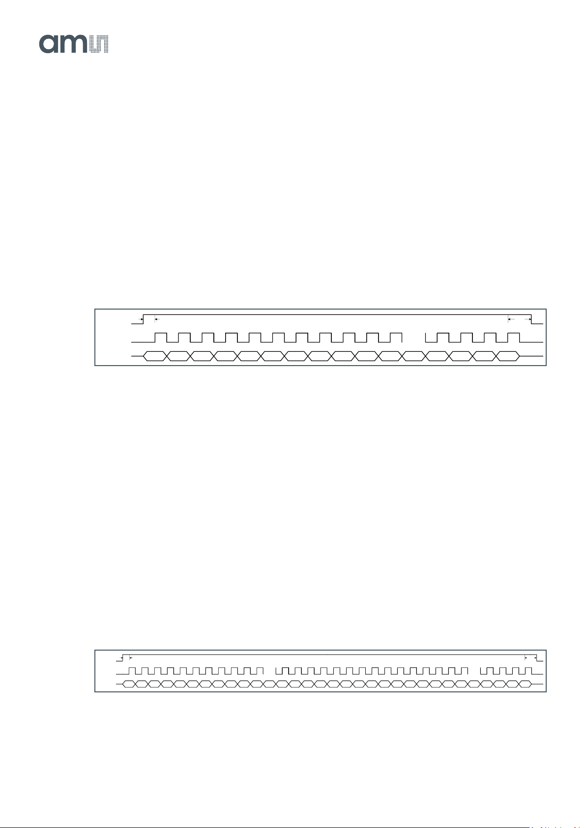
SPI Write
The timing to write data over the SPI interface can be found below.
Figure 15:
SPI Write
The data is sampled by the device on the rising edge of the SPI_CLK and read-in at the last falling
SPI_CLK edge. The SPI_CLK has a maximum frequency of 30 MHz. The SPI_EN signal has to be
high for half a clock period before the first data bit is sampled. SPI_EN has to remain high for one
clock period after the last data bit is sampled.
One write action contains 24 data bits:
● One control bit: First bit to be sent, indicates whether a read (‘0’) or write (‘1’) will occur on the
SPI interface.
● 7 address bits: These bits form the address of the programming register that needs to be
written. The address is sent MSB first.
● 16 data bits: These bits form the actual data that will be written in the register selected with the
address bits. The data is written MSB first.
When several sensor registers need to be written, the timing above can be repeated with SPI_EN
remaining high all the time. See the figure below for an example of 2 registers being written.
Figure 16:
SPI Write of Multiple Registers
SPI_EN
SPI_IN
SPI_CLK
C=’1' A6 A5 A4 A3 A2 A1 A0 D15 D14 D13 ... D3 D2 D1 D0
½ CLK 1 CLK
...
SPI_EN
SPI_IN
SPI_CLK
C=’1' A6 A5 A4 A3 A2 A1 A0 D15 D14 D13 ... D3 D2 D1 D0 C=’1' A6 A5 A4 A3 A2 A1 A0 D15 D14 D13 ... D3 D2 D1 D0
½ CLK 1 CLK
... ...
Document Feedback
CMV12000
Functional Description
Datasheet • PUBLIC
DS000603 • v6-00 • 2023-Sep-22
84 │ 25
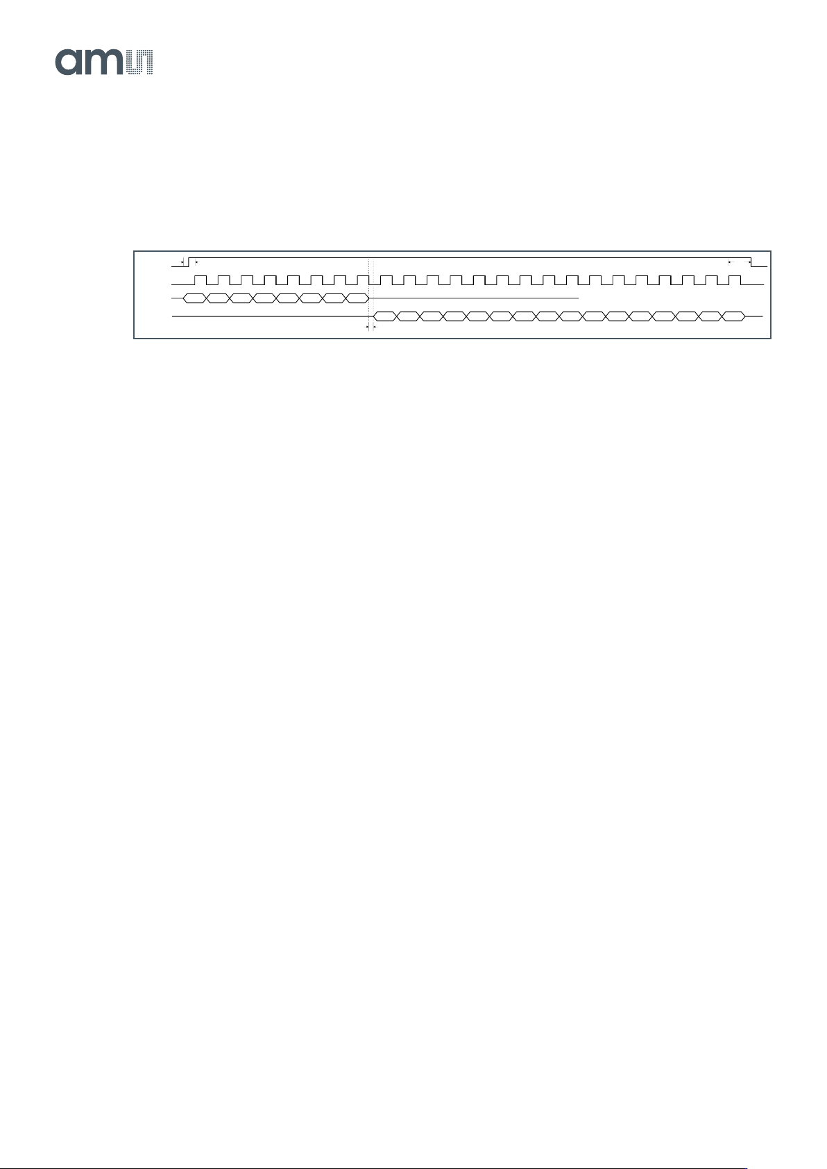
SPI Read
The timing to read data from the registers over the SPI interface can be found below.
Figure 17:
SPI Read
To indicate a read action over the SPI interface, the control bit on the SPI_IN pin is made ‘0’. The
address of the register being read out is sent immediately after this control bit (MSB first). After the
LSB of the address bits, the data is launched on the SPI_OUT pin on the falling edge of the SPI_CLK
with an 8 ns delay (independent of SPI or sensor clock speeds). This means that the data can be
sampled by the receiving system on the rising edge of the SPI_CLK. The data comes over the
SPI_OUT with MSB first.
7.2.8 Requesting a Frame
After starting up the sensor, a number of frames can be requested by sending a FRAME_REQ pulse.
The number of frames can be set by programming the appropriate register (address 80). The default
number of frames to be grabbed is 1.
In internal exposure mode, the exposure time will start after this FRAME_REQ pulse. In the external
exposure mode, the read-out will start after the FRAME_REQ pulse. Both modes are explained into
detail in the sections below.
Internal Exposure Control
In this mode, the exposure time is set by programming the appropriate register (addresses 71-72) of
the device.
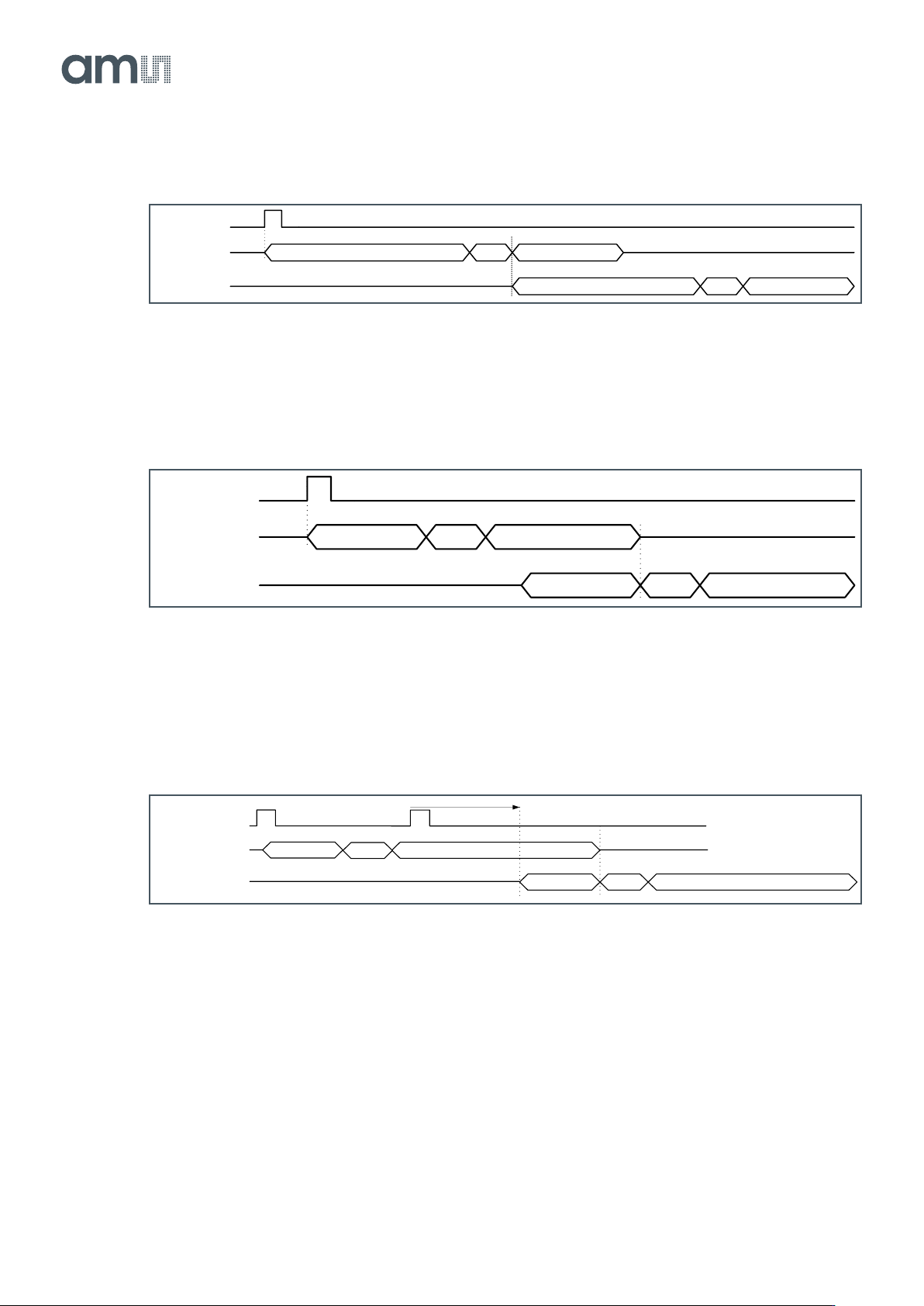
After the high state of the FRAME_REQ pulse is detected, the exposure time will start immediately.
When the exposure time ends (as programmed in the registers), the pixels are being sampled and
prepared for read-out. This sequence is called the frame overhead time (FOT). Immediately after the
FOT, the frame is read out automatically. If more than one frame is requested, the exposure of the
next frame starts already during the read-out of the previous one. See the diagram below for more
details.
SPI_EN
SPI_IN
SPI_CLK
C= 0' A6 A5 A4 A3 A2 A1 A0
D15 D14 D13 D12 D11 D10 D9 D8
SPI_OUT
½ CLK 1 CLK
8ns
D7 D6 D5 D4 D3 D2 D1 D0
Document Feedback
CMV12000
Functional Description
Datasheet • PUBLIC
DS000603 • v6-00 • 2023-Sep-22
84 │ 26
Figure 18:
Internal Exposure Request for Two Frames
When the exposure time is shorter than the read-out time, the FOT and read-out of the next frame will
start immediately after the read-out of the previous frame.
Figure 19:
Internal Exposure Request for Two Frames with Short Exposure Time
When you request a second frame during the read-out of the current frame, the current read-out will
always be finished before the FOT of the new requested frame starts. When the new Frame_REQ
pulse is too early, it will be delayed internally so that the FOT starts immediately after the readout.
Figure 20:
Internal Exposure Delay
If a second frame request is given during the integration of the current frame, the sensor will
remember this and delay the request as described above. This only works up to two Frame_REQ
pulses during integration.
FRAME_REQ
Exposure time
Frame1_cycle
FOT Read-out time
Exposure time
Frame2_cycle
FOT Read-out time
FRAME_REQ
Frame1_cycle
FOT Read-out time
Exposure time
Frame2_cycle
FOT Read-out time
Exposure time
FOT
READOUT
INTE
FOT READOUT
Frame_REQ
INTE
delayed
Current Frame
Next Frame