CMV12000_DS000603_6-00.pdf - 第34页
Document Feedback CMV12000 Functional Description Datasheet • PUBLIC DS000603 • v6 - 00 • 2023 -Sep- 22 84 │ 33 Figure 32 : Pixel Mapping Using 1 × 32 Cha nnels Figure 33 : Pixel Mapping Using 1 × 16 Cha nnels 7.3.5 Cont…
Document Feedback
CMV12000
Functional Description
Datasheet • PUBLIC
DS000603 • v6-00 • 2023-Sep-22
84 │ 32
the register with addresses 92-93. Turning off these channels will reduce the power consumption of
the chip. The amount of rows that will be read out depends on the value in the corresponding register.
By default there are 3072 rows being read out.
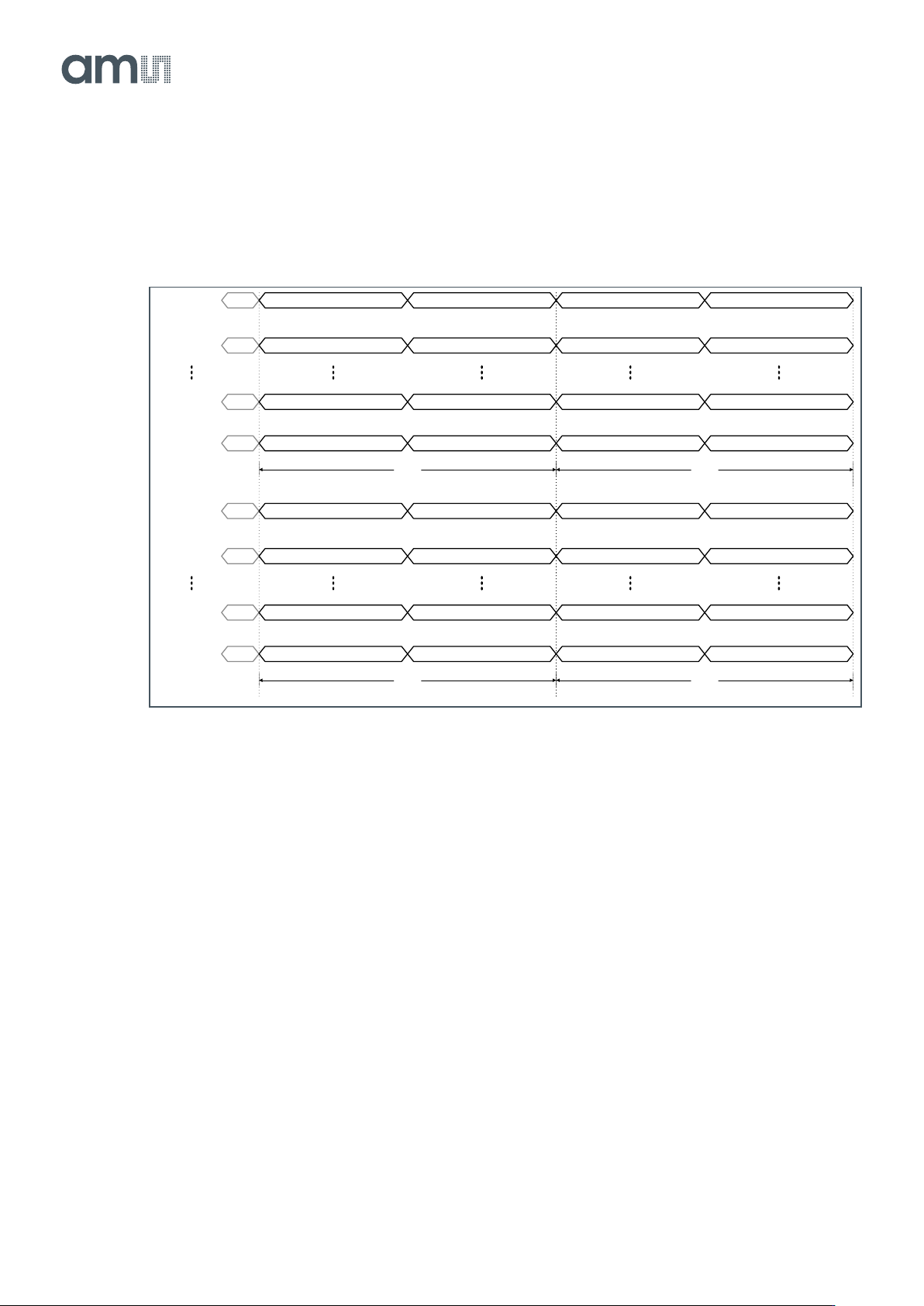
Figure 31:
Pixel Mapping Using 2 x 16 Channels
One Sided Readout Mode
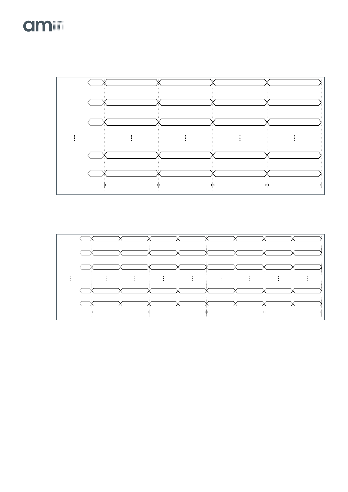
When only one side is used, the pixel data is placed on the outputs as detailed in the figure below
(example of 1 × 32 and 1 × 16). N bursts of 128 pixels happen in parallel on the data outputs. This
means that one complete row is read out in one burst. The rows will be read out following the pattern:
row 1, row 2, row 4, row 3, row 5, row 6, row 8, row 7… So every 3
rd
and 4
th
row are switched.
The time needed to read out two rows is doubled compared to when 64 outputs are used. The top
LVDS channels are not being used in this mode, so they can be turned off by setting the correct bits in
the register with addresses 92-93. Turning off these channels will reduce the power consumption of
the chip. The amount of rows that will be read out depends on the value in the corresponding register.
By default there are 3072 rows read out.
IDLE Pixel 0 to 127Channel 1
IDLEChannel 3
Row 1
Pixel 256 to 383
IDLEChannel 29 Pixel 3584 to 3711
IDLEChannel 31 Pixel 3840 to 3967
Pixel 128 to 255
Pixel 384 to 511
Pixel 3712 to 3839
Pixel 3968 to 4095
IDLE Pixel 0 to 127Channel 33
IDLEChannel 35
Row 2
Pixel 256 to 383
IDLEChannel 61 Pixel 3584 to 3711
IDLEChannel 63 Pixel 3840 to 3967
Pixel 128 to 255
Pixel 384 to 511
Pixel 3712 to 3839
Pixel 3968 to 4095
2x16CH
Pixel 0 to 127
Row 3
Pixel 256 to 383
Pixel 3584 to 3711
Pixel 3840 to 3967
Pixel 128 to 255
Pixel 384 to 511
Pixel 3712 to 3839
Pixel 3968 to 4095
Pixel 0 to 127
Row 4
Pixel 256 to 383
Pixel 3584 to 3711
Pixel 3840 to 3967
Pixel 128 to 255
Pixel 384 to 511
Pixel 3712 to 3839
Pixel 3968 to 4095
Document Feedback
CMV12000
Functional Description
Datasheet • PUBLIC
DS000603 • v6-00 • 2023-Sep-22
84 │ 33
Figure 32:
Pixel Mapping Using 1 × 32 Channels
Figure 33:
Pixel Mapping Using 1 × 16 Channels
7.3.5 Control Channel
The CMV12000 has one LVDS output channel dedicated for the valid data synchronization and timing
of the output channels. The end user must use this channel to know when valid image data or training
data is available on the data output channels.
The control channel transfers status information in 8-bit, 10-bit or 12-bit word format. Every bit of the
word has a specific function. Next table describes the function of the individual bits.
IDLE Pixel 0 to 127Channel 1
IDLEChannel 2
Row 1
Pixel 128 to 255
IDLEChannel 3 Pixel 256 to 383
IDLEChannel 31 Pixel 3840 to 3967
IDLEChannel 32 Pixel 3968 to 4095
Pixel 0 to 127
Row 2
Pixel 128 to 255
Pixel 256 to 383
Pixel 3840 to 3967
Pixel 3968 to 4095
1x32CH
Pixel 0 to 127
Row 4
Pixel 128 to 255
Pixel 256 to 383
Pixel 3840 to 3967
Pixel 3968 to 4095
Pixel 0 to 127
Row 3
Pixel 128 to 255
Pixel 256 to 383
Pixel 3840 to 3967
Pixel 3968 to 4095
IDLE Pixel 0 to 127Channel 1
IDLEChannel 3
Row 1
Pixel 256 to 383
IDLEChannel 5 Pixel 512 to 639
IDLEChannel 29 Pixel 3584 to 3711
IDLEChannel 31 Pixel 3840 to 3967
Pixel 128 to 255
Pixel 384 to 511
Pixel 640 to 767
Pixel 3712 to 3839
Pixel 3968 to 4095
Pixel 0 to 127
Row 2
Pixel 256 to 383
Pixel 512 to 639
Pixel 3584 to 3711
Pixel 3840 to 3967
Pixel 128 to 255
Pixel 384 to 511
Pixel 640 to 767
Pixel 3712 to 3839
Pixel 3968 to 4095
1x16CH
Pixel 0 to 127
Row 4
Pixel 256 to 383
Pixel 512 to 639
Pixel 3584 to 3711
Pixel 3840 to 3967
Pixel 128 to 255
Pixel 384 to 511
Pixel 640 to 767
Pixel 3712 to 3839
Pixel 3968 to 4095
Pixel 0 to 127
Row 3
Pixel 256 to 383
Pixel 512 to 639
Pixel 3584 to 3711
Pixel 3840 to 3967
Pixel 128 to 255
Pixel 384 to 511
Pixel 640 to 767
Pixel 3712 to 3839
Pixel 3968 to 4095
Document Feedback
CMV12000
Functional Description
Datasheet • PUBLIC
DS000603 • v6-00 • 2023-Sep-22
84 │ 34
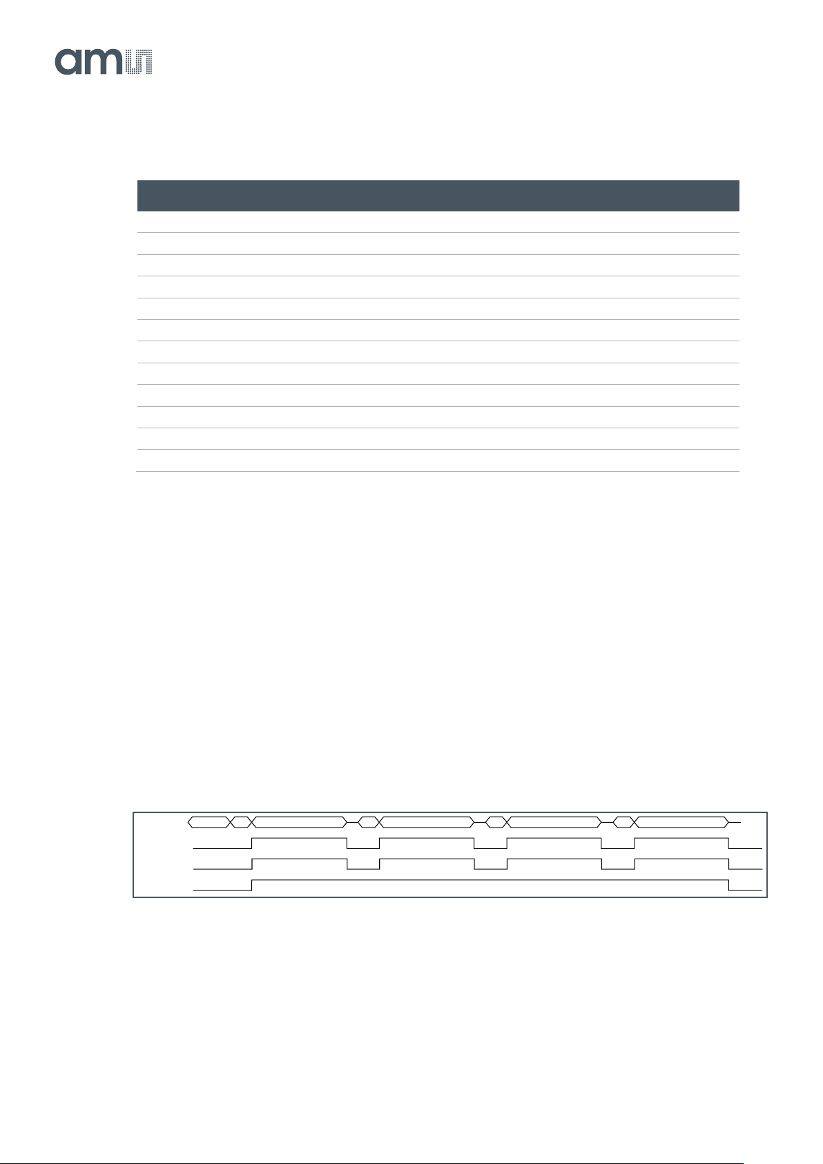
Figure 34:
Control Channel Status Bits
Bit
Function
Description
[0]
DVAL
Indicates valid pixel data on the outputs
[1]
LVAL
Indicates the validity of the read-out of a row
[2]
FVAL
Indicates the validity of the read-out of a frame
[3]
FOT
Indicates when the sensor is in FOT (sampling of image data in pixels)
(1)
[4]
INTE1
Indicates when pixels of integration block 1 are integrating
(1)
[5]
INTE2
Indicates when pixels of integration block 2 are integrating
(1)
[6]
‘0’
Constant zero
[7]
‘1’
Constant one
[8]
‘0’
Constant zero
[9]
‘0’
Constant zero
[10]
‘0’
Constant zero
[11]
‘0’
Constant zero
(1) These status bits are purely functional and are not required to know if the pixel data is valid. DVAL, LVAL and FVAL is
sufficient to know when to sample the image data.
The status bits of the control channel can be monitored on the TDIG1/2 pins (G26/G27) to see the
state of the sensor. See section 7.6.6 for more details.
DVAL, LVAL and FVAL
The first three bits of the control word must be used to identify valid data and the read-out status. The
next figure shows the timing of the DVAL, LVAL and FVAL bits of the control channel with an example
of the read-out of a frame of four rows (default is 3072 rows). This example uses the default mode of
64 outputs (identical for one-side 32 outputs).
Figure 35:
xVAL Timing in 2 × 32 Channel Readout Mode
When only 16 outputs are used per side, the line read-out time is two times longer. The control
channel considers this and the timing in this mode looks like the diagram below. The timing
extrapolates identically for 8, 4, 2 and 1 output(s). Below is an example of a frame of two rows when
only using 16 channels per side.
IDLE OH 128 OH 128 OH 128DATA_OUT
DVAL
LVAL
FVAL
OH 128