CMV12000_DS000603_6-00.pdf - 第59页
Document Feedback CMV12000 Functional Description Datasheet • PUBLIC DS000603 • v6 - 00 • 2023 -Sep- 22 84 │ 58 Attention Subsampling and binning are not s upported when only using one side readout 7.5.2 Training Pattern…
Document Feedback
CMV12000
Functional Description
Datasheet • PUBLIC
DS000603 • v6-00 • 2023-Sep-22
84 │ 57
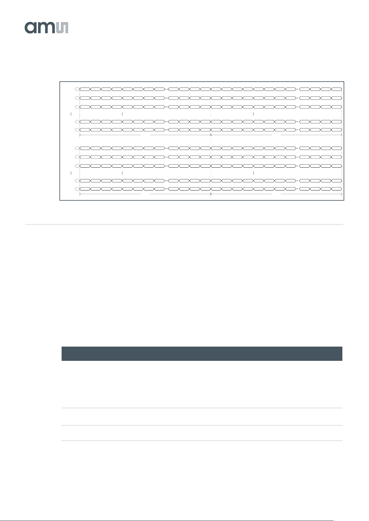
Figure 75:
Pixel Remapping for Color Binning
7.5 Configuring Output Data Format
7.5.1 Output Mode
The number of LVDS channels on each side can be selected by programming the appropriate
sequencer register. The pixel remapping scheme and the read-out timing for each mode can be found
in section 7.3 of this document. See section 7.7 for additional required register settings. The bottom
channels use output pins OUT1_N/P to OUT32_N/P and the top channels use output pins
OUT33_N/P to OUT64_N/P.
Figure 76:
Output Mode
Reg. Name
Address
Bits
Default
Description
Output_mode
81
[4:0]
0
0: 32 outputs used on each side
1: 16 outputs used on each side
3: 8 outputs used on each side
7: 4 outputs used on each side
15: 2 outputs used on each side
31: 1 output used on each side
Disable_top
81
[5]
0
0: Two side readout
1: One side readout (bottom channels only)
Sub_offset
66
[15:0]
0
Set to 65535 when Disable_top = 1 and no subsampling
in Y is used.
IDLE P0 R1Channel 1
IDLEChannel 2
R 1+2+3+4
IDLEChannel 3
IDLEChannel 31
IDLEChannel 32
P1 R2 P0 R3 P1 R4 P62 R1 P63 R2
P64 R1 P65 R2 P64 R3 P65 R4 P126 R1 P127 R2
P128 R1 P129 R2 P128 R3 P129 R4 P190 R1 P191 R2
P1920 R1 P1921 R2 P1920 R3 P1921 R4 P1982 R1 P1983 R2
P1984 R1 P1985 R2 P1984 R3 P1985 R4 P2046 R1 P2047 R2
BOTTOM
TOP
P2 R1 P3 R2 P2 R3 P3 R4 P62 R3 P63 R4
P66 R1 P67 R2 P66 R3 P67 R4 P126 R3 P127 R4
P130 R2 P131 R2 P130 R3 P131 R4 P190 R3 P191 R4
P1922 R1 P1923 R2 P1922 R3 P1923 R4
P1986 R1 P1987 R2 P1987 R3 P1986 R4
P1982 R3 P1983 R4
P2046 R3 P2047 R4
IDLE P0 R2Channel 33
IDLEChannel 34
R 1+2+3+4
IDLEChannel 35
IDLEChannel 63
IDLEChannel 64
P1 R1 P0 R4 P1 R3 P62 R2 P63 R1
P64 R2 P65 R1 P64 R4 P65 R3 P126 R2 P127 R1
P128 R2 P129 R1 P128 R4 P129 R3 P190 R2 P191 R1
P1920 R2 P1921 R1 P1920 R4 P1921 R3 P1982 R2 P1983 R1
P1984 R2 P1985 R1 P1984 R4 P1985 R3 P2046 R2 P2047 R1
P2 R2 P3 R1 P2 R4 P3 R3 P62 R4 P63 R3
P66 R2 P67 R1 P66 R4 P67 R3 P126 R4 P127 R3
P130 R2 P131 R1 P130 R4 P131 R3 P190 R4 P191 R3
P1922 R2 P1923 R1 P1922 R4 P1923 R3
P1986 R2 P1987 R1 P1986 R4 P1987 R3
P1982 R4 P1983 R3
P2046 R4 P2047 R3
P0 R5
R 5+6+7+8
P1 R6 P0 R7 P1 R8 P62 R5 P63 R6
P64 R5 P65 R6 P64 R7 P65 R8 P126 R5 P127 R6
P128 R5 P129 R6 P128 R7 P129 R8 P190 R5 P191 R6
P1920 R5 P1921 R6 P1920 R7 P1921 R8 P1982 R5 P1983 R6
P1984 R5 P1985 R6 P1984 R7 P1985 R8 P2046 R5 P2047 R6
P2 R5 P3 R6 P2 R7 P3 R8 P62 R7 P63 R8
P66 R5 P67 R6 P66 R7 P67 R8 P126 R7 P127 R8
P130 R5 P131 R6 P130 R7 P131 R8 P190 R7 P191 R8
P1922 R5 P1923 R6 P1922 R7 P1923 R8
P1986 R5 P1987 R6 P1987 R7 P1986 R8
P1982 R7 P1983 R8
P2046 R7 P2047 R8
P0 R6
R 5+6+7+8
P1 R5 P0 R8 P1 R7 P62 R6 P63 R5
P64 R6 P65 R5 P64 R8 P65 R7 P126 R6 P127 R5
P128 R6 P129 R5 P128 R8 P129 R7 P190 R6 P191 R5
P1920 R6 P1921 R5 P1920 R8 P1921 R7 P1982 R6 P1983 R5
P1984 R6 P1985 R5 P1984 R8 P1986 R7 P2046 R6 P2047 R5
P2 R6 P3 R5 P2 R8 P3 R7 P62 R8 P63 R7
P66 R6 P67 R5 P66 R8 P67 R7 P126 R8 P127 R7
P130 R6 P131 R5 P130 R8 P131 R7 P190 R8 P191 R7
P1922 R6 P1923 R5 P1922 R8 P1923 R7
P1986 R6 P1987 R5 P1986 R8 P1987 R7
P1982 R8 P1983 R7
P2046 R8 P2047 R7
Document Feedback
CMV12000
Functional Description
Datasheet • PUBLIC
DS000603 • v6-00 • 2023-Sep-22
84 │ 58
Attention
Subsampling and binning are not supported when only using one side readout
7.5.2 Training Pattern
As detailed in section 7.3.6, a training pattern is sent over the LVDS data channels whenever no valid
image data is sent. The training pattern TP1 can be programmed using the sequencer register below.
Figure 77:
Training Pattern
Reg. Name
Address
Bits
Default
Description
Training_pattern
89
[11:0]
85
Sets the training pattern value.
7.5.3 Bit Mode
The CMV12000 has the possibility to send 12 bits, 10 bits or 8 bits per pixel. The end user can select
the desired resolution by programming the corresponding sequencer register. See section 7.2.6 for
details on how the bit mode can be changed. See section 7.7 for additional required register settings.
Figure 78:
Bit Mode Setting
Reg. Name
Address
Bits
Default
Description
Bit_mode
118
[1:0]
1
0: 12b (12 bits per pixel)
1: 10b (10 bits per pixel)
2: 8b (8 bits per pixel)
When changing the bit mode of the ADC, the ADC input range also has to be modified so the analog
pixel voltage is in the correct range of the ADC input.
Figure 79:
ADC Range Settings
Reg. Name
Address
Bits
Default
Description
ADC_range
116
[7:0]
127
Change the slope and the input range of the ramp used
by the ADC
205: 8b
165: 10b
230: 12b
Document Feedback
CMV12000
Functional Description
Datasheet • PUBLIC
DS000603 • v6-00 • 2023-Sep-22
84 │ 59
Reg. Name
Address
Bits
Default
Description
ADC_range_mult
116
[9:8]
1
Change multiplier of the slope and the input range of the
ramp used by the ADC
0: 8b (x1)
1: 10b (x2)
3: 12b (x4)
ADC_range_mult2
100
[1:0]
0
Change multiplier of the slope and the input range of the
ramp used by the ADC for lower clock speeds. Only use
with ADC_range_mult=3.
0: x4
1: x8
3: x16
The ADC range also has to be adjusted when using different clock speeds. See section 7.7.4.
7.5.4 Data Rate
During start-up or after a sequencer reset, the data rate can be changed if a lower speed than
600 Mbit/s is desired. This can be done by applying a lower LVDS input clock (LVDS_CLK_P/N).
7.5.5 Power Consumption
The power consumption of the sensor can be decreased by disabling the LVDS data channels when
they are not used (in 32, 16, 8, 4, 2 or 1 channel(s) mode). Disabling an output saves about 15 mW on
the VDD18 supply per output.
Figure 80:
Power Consumption
Reg. Name
Address
Bits
Default
Description
Channel_en_bot
90
91
[15:0]
[15:0]
65535
Sets 1 channel per bit for the bottom outputs
0: Disabled
1: Enabled
Channel_en_top
92
93
[15:0]
[15:0]
65535
Sets 1 channel per bit for the top outputs
0: Disabled
1: Enabled
Channel_en
94
[2:0]
7
Bit 0: Output clock channel
Bit 1: Control channel
Bit 2: Input clock channel
0: Disabled
1: Enabled