CMV12000_DS000603_6-00.pdf - 第24页
Document Feedback CMV12000 Functional Description Datasheet • PUBLIC DS000603 • v6 - 00 • 2023 -Sep- 22 84 │ 23 The LVDS input clock should only start after the rise time of the supplies. The e xternal reset pin should b…
Document Feedback
CMV12000
Functional Description
Datasheet • PUBLIC
DS000603 • v6-00 • 2023-Sep-22
84 │ 22
Pin Name
Description
LVDS_CLK_P/N
Input clock, frequency range between 100 MHz and 600 MHz, depending on the bit mode.
SYS_RES_N
System reset pin, active low signal. Resets the on-board sequencer and must be kept low
during start-up.
FRAME_REQ
Frame request pin. When a high state is detected on this pin, the programmed number of
frames is captured and sent by the sensor. The pulse should be at least 8, 10 or 12 * LVDS
input clock periods wide to be detected, depending on the used bit mode.
SPI_IN
Data input pin for the SPI interface. The data to program the image sensor is sent over this
pin.
SPI_EN
SPI enable pin. When this pin is high, the data should be written/read on the SPI.
SPI_CLK
SPI clock. This is the clock on which the SPI runs (max 30 MHz).
T_EXP1
Input pin, which can be used to program the exposure time externally. The pulse should be
at least 8, 10 or 12 * LVDS input clock periods wide to be detected, depending on the used
bit mode. Optional.
T_EXP2
Input pin, which can be used to program the exposure time externally in interleaved high
dynamic range mode. The pulse should be at least 8, 10 or 12 * LVDS input clock periods
wide to be detected, depending on the used bit mode. Optional.
7.2.4 Clocking
The LVDS input clock defines the output data rate of the CMV12000. The maximum data rate of the
output is 600 Mbit/s (DDR 300 MHz output clock) which results in an input LVDS_CLK clock of
600 MHz. The minimum LVDS_CLK_P/N frequency is 100 MHz for 12-bit, 10-bit and 8-bit. At lower
frequencies, image performance will decrease. Any input frequency (min < f < max) applied (in MHz)
will result in a corresponding output data rate (in Mbit/s). Some register settings need to be changed
when changing the input clock frequency from 600 MHz. See section 7.7.4.
7.2.5 Startup Sequence
The following sequence should be followed when the device is started up:
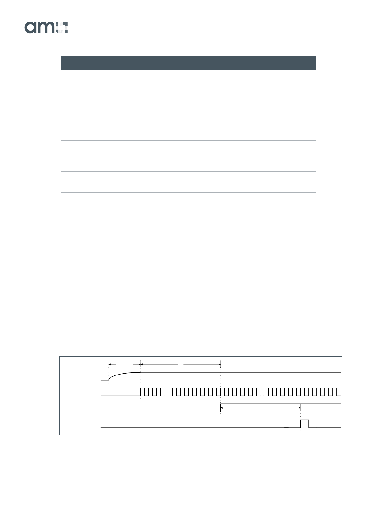
Figure 12:
Startup Sequence
1μs
1μs
Stable time
Supply
LVDS_CLK
SYS_RES_N
FRAME_REQ
Document Feedback
CMV12000
Functional Description
Datasheet • PUBLIC
DS000603 • v6-00 • 2023-Sep-22
84 │ 23
The LVDS input clock should only start after the rise time of the supplies. The external reset pin
should be released at least 1 μs after the supplies have become stable. The first frame can be
requested 1 μs after the reset pin has been released. An optional SPI upload (to program the
sequencer) is possible 1 μs after the reset pin has been released. In this case, the FRAME_REQ
pulse must be postponed until after the SPI upload has been completed.
7.2.6 Reset Sequence
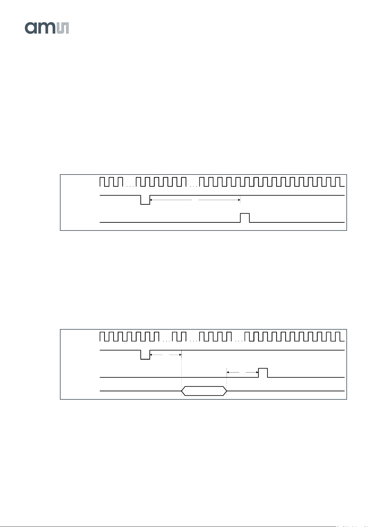
If a sensor reset is necessary while the sensor is running, the next sequence should be followed:
Figure 13:
Reset Sequence
The on-board sequencer will be reset and all programming registers will return to their default start-up
values when a falling edge is detected on the SYS_RES_N pin. After the reset there is a minimum
time of 1 μs needed, before a FRAME_REQ pulse can be sent.
When a switch from 12-bit to 10-bit or 8-bit mode (or vice versa) is necessary, the following sequence
should be followed:
Figure 14:
Reset Sequence with Changing Bit Mode
The following SPI register should be uploaded in this mode: Bit_mode (address 118): set to desired bit
resolution mode.
1μs
LVDS_CLK
SYS_RES_N
FRAME_REQ
1μs
LVDS_CLK
SYS_RES_N
FRAME_REQ
Bit mode settings
SPI upload
1μs
Document Feedback
CMV12000
Functional Description
Datasheet • PUBLIC
DS000603 • v6-00 • 2023-Sep-22
84 │ 24
7.2.7 SPI Programming
Programming the sensor is done by writing the appropriate values to the on-board registers. These
registers can be written over a simple serial interface (SPI). The details of the timing and data format
are described below. The data written to the programming registers can also be read out over this
same SPI interface.
SPI I/O’s are pulled low when not used/enabled.
SPI Write
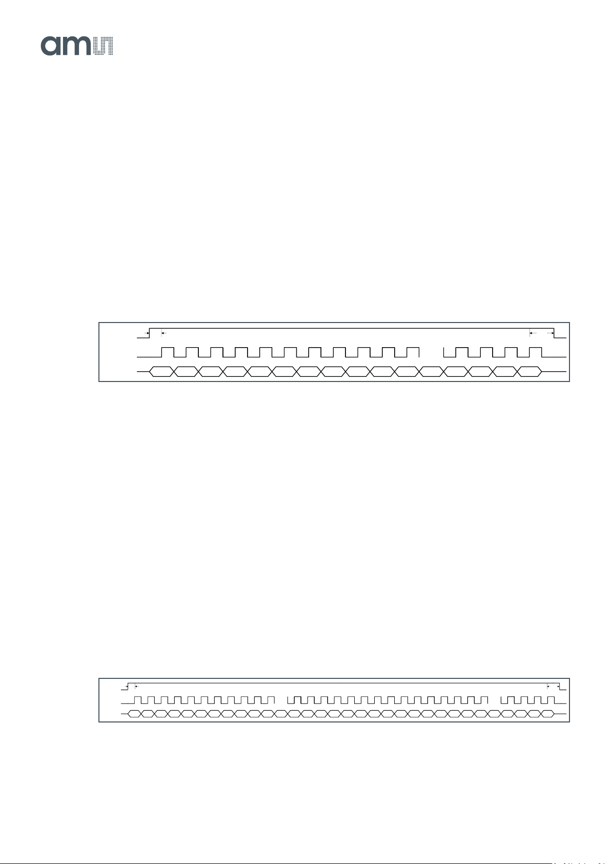
The timing to write data over the SPI interface can be found below.
Figure 15:
SPI Write
The data is sampled by the device on the rising edge of the SPI_CLK and read-in at the last falling
SPI_CLK edge. The SPI_CLK has a maximum frequency of 30 MHz. The SPI_EN signal has to be
high for half a clock period before the first data bit is sampled. SPI_EN has to remain high for one
clock period after the last data bit is sampled.
One write action contains 24 data bits:
● One control bit: First bit to be sent, indicates whether a read (‘0’) or write (‘1’) will occur on the
SPI interface.
● 7 address bits: These bits form the address of the programming register that needs to be
written. The address is sent MSB first.
● 16 data bits: These bits form the actual data that will be written in the register selected with the
address bits. The data is written MSB first.
When several sensor registers need to be written, the timing above can be repeated with SPI_EN
remaining high all the time. See the figure below for an example of 2 registers being written.
Figure 16:
SPI Write of Multiple Registers
SPI_EN
SPI_IN
SPI_CLK
C=’1' A6 A5 A4 A3 A2 A1 A0 D15 D14 D13 ... D3 D2 D1 D0
½ CLK 1 CLK
...
SPI_EN
SPI_IN
SPI_CLK
C=’1' A6 A5 A4 A3 A2 A1 A0 D15 D14 D13 ... D3 D2 D1 D0 C=’1' A6 A5 A4 A3 A2 A1 A0 D15 D14 D13 ... D3 D2 D1 D0
½ CLK 1 CLK
... ...