M3plus_OperationManual_e.pdf - 第81页
3 - 16 3 Creating the PCB data 3. Creating the PCB information 3 Check the message and press the [OK] button. c CAUTION Data that has undergone block distribution cannot be restored to the original state. 4 Check the dis…
3 -15
3
Creating the PCB data
3. Creating the PCB information
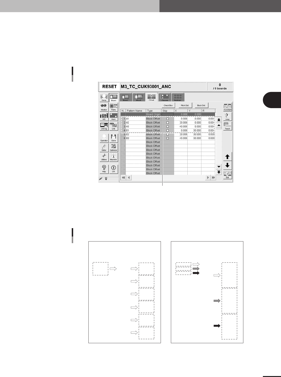
3.3.2 Block distribution function
This function copies the mount data for the reference block and distributes it over all
other blocks. The distributed mount data is automatically entered and displayed on the
mount information screen according to the blocks or mount data.
1
Check the block offset data.
At least one item of block offset data must have been entered to perform the "block
distribution" function.
Checking the block offset data
At least one item of block offset data must have been entered.
27317-5E-20
2
Press the [Block Disp.] button and select the type of block
distribution.
Pressing the [Block Disp.] button opens a dialog box for selecting the type of block
distribution. Select "Block Repeat" or "Column Repeat" and press the [OK] button.
All mount data are copied and distributed
over each block, and then displayed according
to the blocks.
Before distribution After distribution
Before distribution After distribution
P01
P02
P03
1
2
3
4
5
6
7
8
9
10
11
12
13
14
15
16
17
18
P01
P02
P03
1
2
3
4
5
6
7
8
9
10
11
12
13
14
15
16
17
18
P01
P01
P01
P01
P01
P01
P02
P02
P02
P02
P02
P02
P03
P03
P03
P03
P03
P03
1
2
3
4
5
6
7
8
9
10
11
12
13
14
15
16
17
18
P01
P02
P03
P01
P02
P03
P01
P02
P03
P01
P02
P03
P01
P02
P03
P01
P02
P03
1
2
3
4
5
6
7
8
9
10
11
12
13
14
15
16
17
18
Mount data in each row is sequentially copied
and distributed over each block, and then
displayed according to the mount data.
"Block Repeat"
"Column Repeat"
Block distribution type
23432-5E-20
3 -16
3
Creating the PCB data
3. Creating the PCB information
3
Check the message and press the [OK] button.
c
CAUTION
Data that has undergone block distribution cannot be restored to the original state.
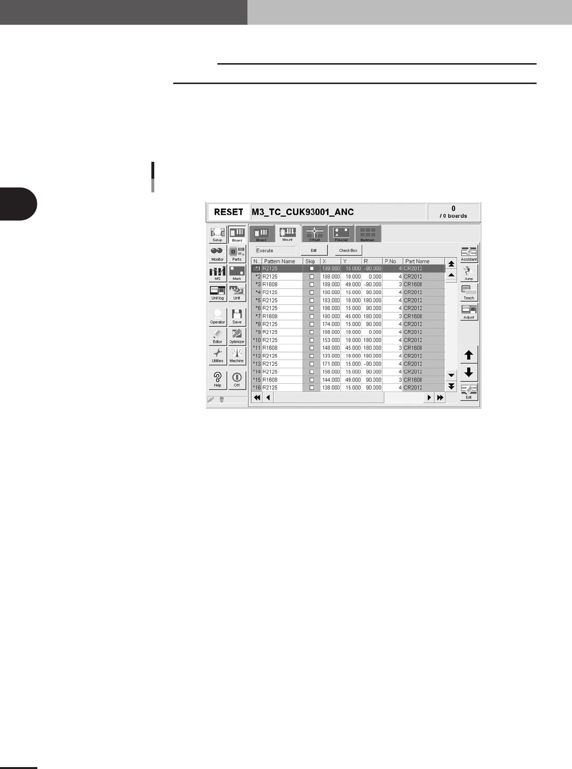
4
Check the distributed block offset data.
After block distribution is complete, the block offset data distributed for mount
information is displayed, so check the offset data. The "Skip" check boxes are all
cleared after block distribution. If there are blocks where you want to skip mounting
components, press the [Check Box] button and then mark the "Skip" check box.
Block offset data after block distribution
Example of "Block Repeat" distribution type
27318-5E-20
3 -17
3
Creating the PCB data
3. Creating the PCB information
3.4 Fiducial parameters
The fiducial function corrects local distortion or warps on a PCB that may occur from
errors in machining the PCB outline and locate pin holes, PCB clamping mechanism
fluctuations, using recognition results of the fiducial marks provided on the PCB.
Selecting the [Fiducial] tab opens the screen for setting fiducial mark parameters and
their coordinates. Set these parameters as explained below when using the fiducial
function. (See "3.4.1" to "3.4.3" in this section for more details.) Two or four fiducial
marks are used as a set, but it is okay if each mark is different in shape. Fiducial mark
data must be registered in the mark information beforehand. (See "5. Creating the mark
information" in this chapter.)
Fiducial parameter
4
1
56 879
2
3
Fiducial parameter
27409-5E-20
1 Board, Block, Local
Fiducial functions are broadly classified into three types: "Board" fiducial function specified for a
PCB, "Block" fiducial function specified for each block of a multi-block PCB, and "Local" fiducial
function related to mounting data. The fiducial function you wan to use should be set to "Execute".
To change the setting, press the [Edit] button on the right end.
2 Board
On the top line of the parameter list, set the board fiducial mark data.
3 Block
On the second line of the parameter list, set the block fiducial mark data.
4 Pattern Name
Enter the fiducial mark name here. (Names cannot be entered in the top and second rows.)
5 Type
On the third or subsequent lines, specify the type of fiducial function you want to use, by selecting
from among ""Point", "Local", "4Local-M" and "4Local-S".
6 X1, Y1
Enter the XY coordinates of Mark 1 relative to the PCB origin in millimeter. You can perform
teaching with the [Teach] button.
7 Mark 1
Enter the mark No. for Mark 1 (mark No. registered as fiducial mark in the mark information).
8 X2, Y2
Enter the XY coordinates of Mark 2 relative to the PCB origin in millimeter. You can perform
teaching with the [Teach] button.