D系列电路图00194841-02_DC_SIPLACED12_DE+EN.pdf - 第138页
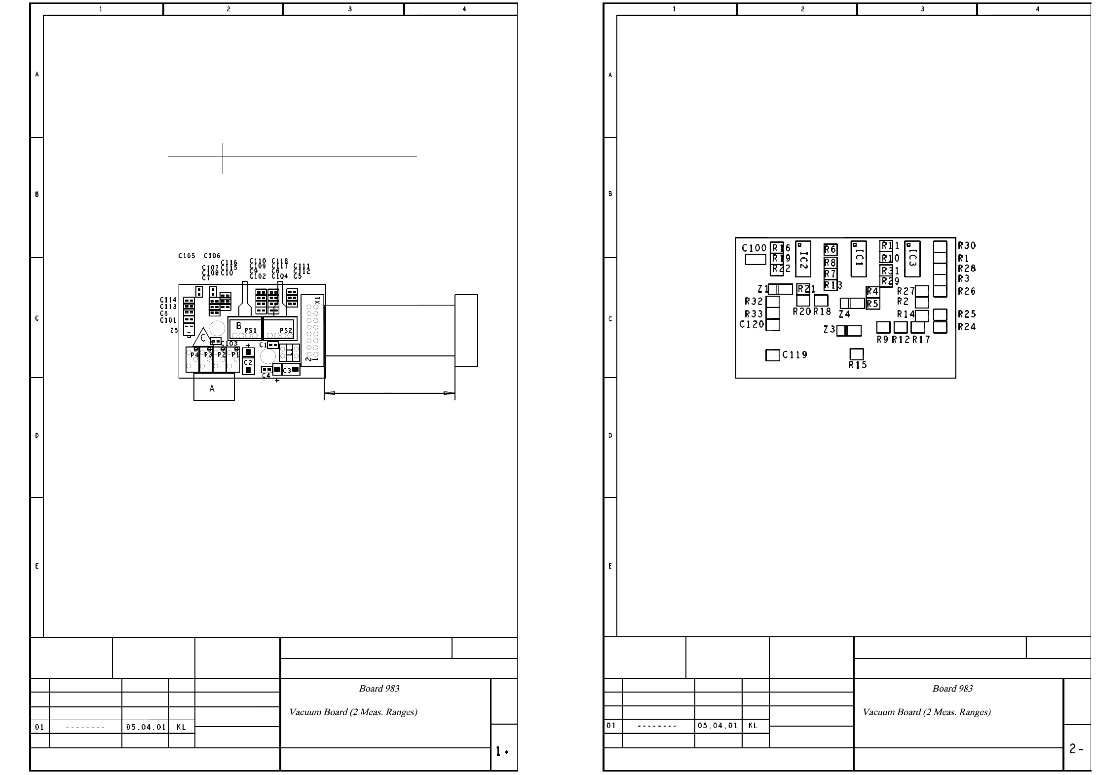
5 - 17 0036373 8-020 101ND4 Leiter platte 983, V a kuumpla tine (2 B ereiche ) (Bl. 1 v . 2) PCB 98 3, vacuum b oard (2 mea s. rang es) (sh. 1 of 2) 0036373 8-020 101ND4 Leiter platte 983, V a kuumpla tine (2 B ereiche )…
5 - 16
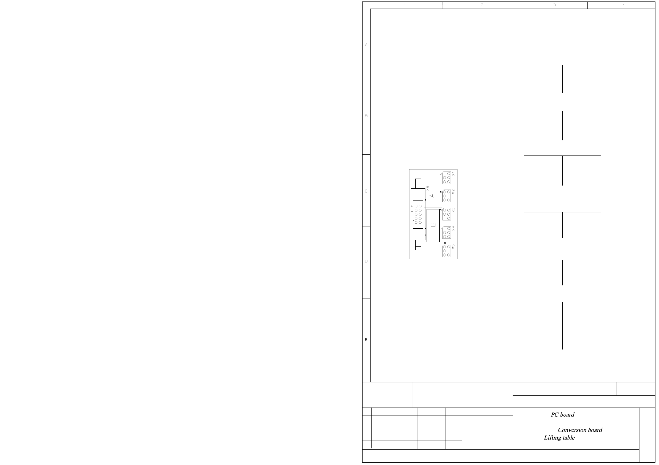
00362766-010101ND4 Leiterplatte, Umsetzplatine Hubtisch
PCB, conversion board, lifting table
Stat.
01
Modified
04.04.01
Date
KD
Name
PC board
Dorfner
04.04.01
Date
Name
Component layout, component side
G32918 - N0032 - U201 - * - 17 00362766-010101ND4
Scale
1 : 1
1 -
Sheet
984
2-layer
A Assembly designation 11x13 (solder side)
B Inspection label (solder side)
1
2
3
6
2
3
4
6
2
3
5
6
1
2
3
6
2
3
4
6
1
2
3
4
5
6
10
Connector X1
Connector X2
Connector X3
Connector X4
Connector X5
Connector X6
Key
Track A
+24V
GND
Key
Track B
+24V
GND
Key
+24V
Limit switch
GND
GND
+24V
Valve "up"
Key
GND
+24V
Valve "down"
Key
+24V
Track A
Track B
Limit switch
Valve "up"
Valve "down"
GND
pflichten zu Schadenersatz. Alle Rechte vorbehalten, ins
besondere für den Fall der Patenterteilung oder GM-Eintragung
wertung und Mitteilung ihres Inhalts nicht gestattet, soweit
Weitergabe sowie Vervielfältigung dieser Unterlage,Ver-
nicht ausdrücklich zugestanden. Zuwiderhandlungen ver-
Proprietary date, company confidential. All rights reserved.
Confie a titre de secret d'entreprise. Tous droits reserves.
Confiado como secrete industrial. Nos reservamos todos los derechos.
Comunicado como segredo empresarial. Reservados todos os direitos.
SIPLACE D1/D2
SIEMENS AG
Copyright reserved
DT EA
Leiterplatte /
Umsetzplatine /
Hubtisch /
Bestückungsplan, Bauteilseite
5 - 17
00363738-020101ND4 Leiterplatte 983, Vakuumplatine (2 Bereiche) (Bl. 1 v. 2)
PCB 983, vacuum board (2 meas. ranges) (sh. 1 of 2)
00363738-020101ND4 Leiterplatte 983, Vakuumplatine (2 Bereiche) (Bl. 2 v. 2)
PCB 983, vacuum board (2 meas. ranges) (sh. 2 of 2)
pflichten zu Schadenersatz. Alle Rechte vorbehalten, ins
besondere für den Fall der Patenterteilung oder GM-Eintragung
wertung und Mitteilung ihres Inhalts nicht gestattet, soweit
Weitergabe sowie Vervielfältigung dieser Unterlage,Ver-
nicht ausdrücklich zugestanden. Zuwiderhandlungen ver-
Proprietary date, company confidential. All rights reserved.
Confie a titre de secret d'entreprise. Tous droits reserves.
Confiado como secrete industrial. Nos reservamos todos los derechos.
Comunicado como segredo empresarial. Reservados todos os direitos.
00363738-020101ND4
G32918-N0031-U501-*-0017
C = ESD-LABEL
B = INSPECTION LABEL ON PRESSURE SENSORS
A = IDENTIFICATION LABEL, LATERAL TO P1-P4
Sheet
X1
Connector
X10 head adapter DLM-X, 03019066
Assembly
KLOSE
05.04.01
Placement diagram component side
4-layer PCB
Scale 1:1
Name
Date
Name
Date
Note
Status
Copyright reserved
SIEMENS AG
DT EA
Leiterplatte 983 /
Vakuumplatine (2 Bereiche) /
SIPLACE D1/D2
pflichten zu Schadenersatz. Alle Rechte vorbehalten, ins
besondere für den Fall der Patenterteilung oder GM-Eintragung
wertung und Mitteilung ihres Inhalts nicht gestattet, soweit
Weitergabe sowie Vervielfältigung dieser Unterlage,Ver-
nicht ausdrücklich zugestanden. Zuwiderhandlungen ver-
Proprietary date, company confidential. All rights reserved.
Confie a titre de secret d'entreprise. Tous droits reserves.
Confiado como secrete industrial. Nos reservamos todos los derechos.
Comunicado como segredo empresarial. Reservados todos os direitos.
G32918-N0031-U501-*-0017
00363738-020101ND4
05.04.01
KLOSE
Status
Note
Date
Date
Name
Name
Placement diagram component side
4-layer PCB
Scale 1:1
Sheet
Copyright reserved
SIEMENS AG
DT EA
Vakuumplatine (2 Bereiche) /
Leiterplatte 983 /
SIPLACE D1/D2
5 - 18
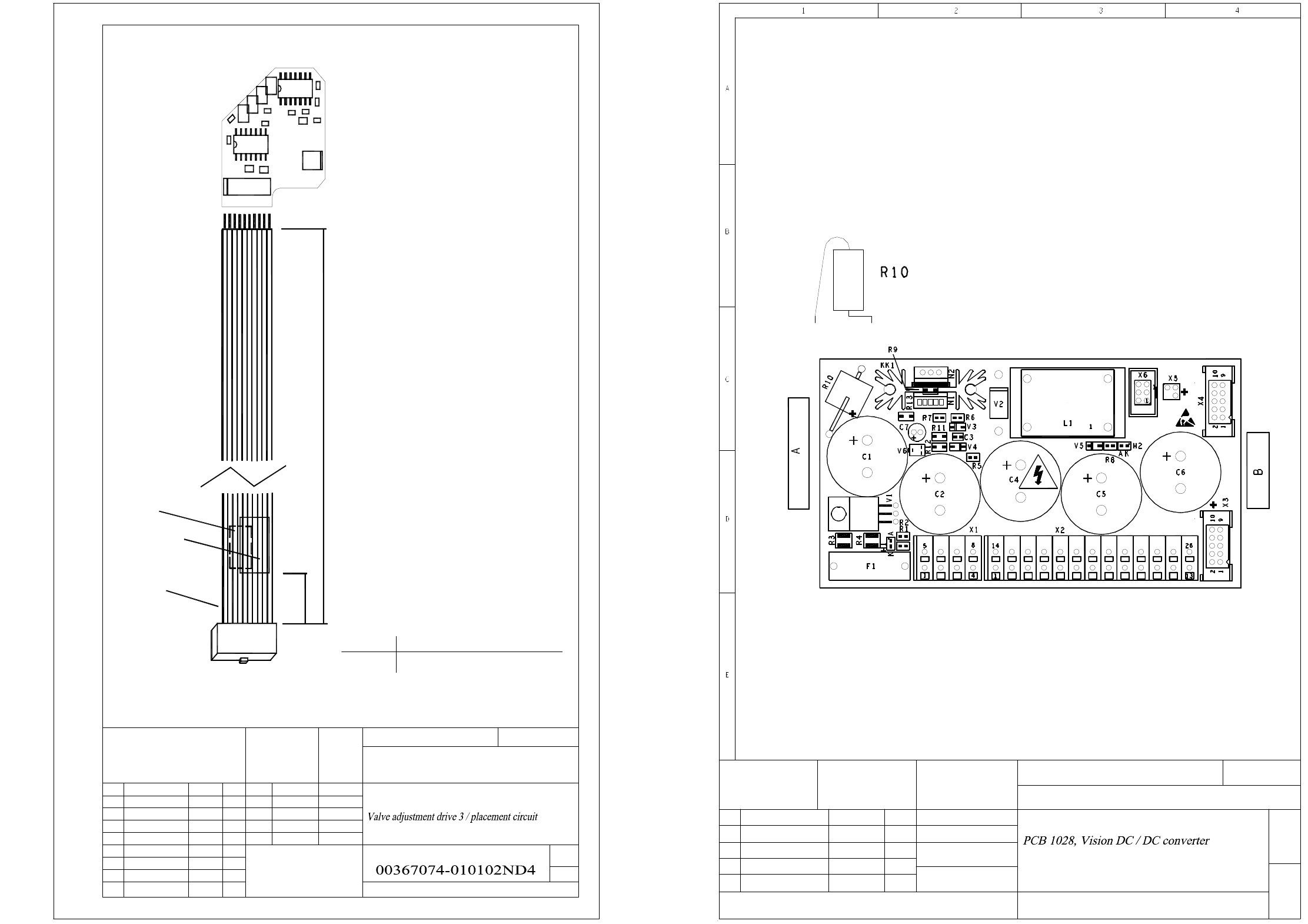
00367074-010102ND4 Vertilstelleinheit 3 / Bestückkreis
Adjustment unit 3, placement circuit
03002280-030101ND4 Leiterplatte 1028 / Vision DC/DC-Konverter
PCB 1028, vision DC / DC converter
Stat. NameDate
06.11.2001
Standard
Checked
Drawn
Date
Item name / Benennung
Document no. / Unterlagen-Nr. (-FS RS US UA SP F)
Name
Scale / Maßstab
Sheet
1
1
Sh.
Format A4
a patent or the registration of a utility model or design.
damages. All rights are reserved in the event of the grant of
out express authority. Offenders are liable to the payment of
or communication of the contents thereof, are forbidden with-
Copying of this document, and giving it to others and the use
Replacement for
Copyright reserved
C4
C2
354.0mm
-5.0mm
Cable, 05-1630-5
B1, B2
Pin 1
A1
X1
50.0mm
C5
R3
R
1
X1
1
C3
+5.0mm
R2
10
R5
U2
R6
R4
U3
R7
X2
X4
X5
X3
U1
C6
readable, when X1 is on the left.
AFO and WIP inspection labels.
50mm distance from cable end.
Readable, when X1 is on the right.
X18 stepping motor board 00344488
May be printed
On the back.
Label position:
on the cable
AssemblyConnector
X1
B1, B2:
Identification label,
A1:
US02 402386 06.03.06 TB
SIPLACE D1/D2
Ventilstelleinheit 3 / Bestückkreis
besondere für den Fall der Patenterteilung oder GM-Eintragung
pflichten zu Schadenersatz. Alle Rechte vorbehalten, ins
nicht ausdrücklich zugestanden. Zuwiderhandlungen ver-
wertung und Mitteilung ihres Inhalts nicht gestattet, soweit
Weitergabe sowie Vervielfältigung dieser Unterlage,Ver-
DT EA
SIEMENS AG
Mayerhofer
Modified
Stat.
04.
Modified
25.09.06
Date
KD
Name
SIEMENS AG
DT EA
Date
Name
21.01.02
KLOSE
G32905 - N0117 - U021 - * - 0017
03002280-030101ND4
Leiterplatte 1028, Vision DC/DC-Konverter
2-LAYER PCB
COMPONENT LAYOUT, COMPONENT SIDE
Scale 1 : 1
Sheet
1 -
C = ESD label
Glue "lightning" label on C4
B = inspection label on C6
A = identification label on C1
pflichten zu Schadenersatz. Alle Rechte vorbehalten, ins
besondere für den Fall der Patenterteilung oder GM-Eintragung
wertung und Mitteilung ihres Inhalts nicht gestattet, soweit
Weitergabe sowie Vervielfältigung dieser Unterlage,Ver-
nicht ausdrücklich zugestanden. Zuwiderhandlungen ver-
Proprietary date, company confidential. All rights reserved.
Confie a titre de secret d'entreprise. Tous droits reserves.
Confiado como secrete industrial. Nos reservamos todos los derechos.
Comunicado como segredo empresarial. Reservados todos os direitos.
Copyright reserved
SIPLACE D1/D2