Tracker-2800-2800S.pdf - 第66页
66 Suggestions to minimiz e effects on bipolar transistors: 1. Use 5 Volts or less for testing the base-emitte r or collector-emitter. 2. If using 8 Volts or greater, th en keep the duration of the test as short as possi…
65
4-2. TRANSISTORS
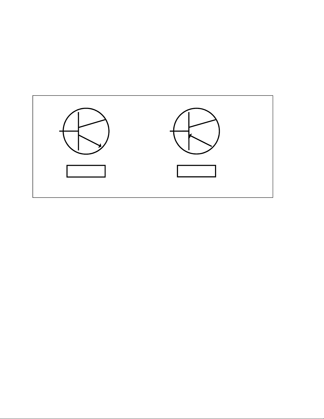
A bipolar transistor is a three layer device. There are two basic types. A PNP transistor has a layer of
n-type silicon material sandwiched between two layers of p-type material. An NPN transistor has a
layer of p-type silicon material sandwiched between two layers of n-type material. Figure 4-18 shows
the relationship between type of material and circuit symbol for a PNP and an NPN transistor.
Figure 4-18. Diagram of an NPN and PNP Bipolar Transistor.
IMPORTANT NOTE
Use of this instrument may alter the current gain (h
FE
or ß) of a bipolar transistor whenever the emitter
is tested. Either the base-emitter or collector-emitter test circuits satisfy this criterion. While heating of
the device due to the current produced by the instrument may cause a temporary change in h
FE
(most
noticeable in the low range), a permanent shift in h
FE
may occur whenever the base-emitter junction is
forced into reverse breakdown (~8-20 Volts). If the voltage is above 8 Volts, then the magnitude of the
shift depends on the duration of the test and the resistance selected. Reducing the voltage to 5 Volts or
less will avoid this problem.
Most bipolar transistor circuit designers take into account a wide variation in h
FE
as a normal
occurrence and design the related circuitry to function properly over the expected range of h
FE
. The
effects mentioned above are for the most part much smaller than the normal device variation so that the
use of this instrument will have no effect on the functionality of good devices and can fulfill its
intended purpose of a means to locate faulty components. However, some circuits may depend on the
h
FE
of the particular part in use, e.g. instrumentation that is calibrated to certain h
FE
value, or precision
differential amplifiers with matched transistors. In such instances, this instrument should not be used
on the base-emitter junction as it may cause the h
FE
to shift outside the limited range where calibration
can correct for any change.
PNP
NPN
E
E
B
B
C
NPN PNP
BASE
COLLECTOR
EMITTER
BASE
EMITTER
C
COLLECTOR
66
Suggestions to minimize effects on bipolar transistors:
1. Use 5 Volts or less for testing the base-emitter or collector-emitter.
2. If using 8 Volts or greater, then keep the duration of the test as short
as possible.
3. Identify the base, emitter and collector pins of the device and then test
the collector-base junction to determine whether it is an NPN or PNP.
Since the emitter is not tested there will be no effect on h
FE
regardless of the selected voltage.
Bipolar Transistor Signatures
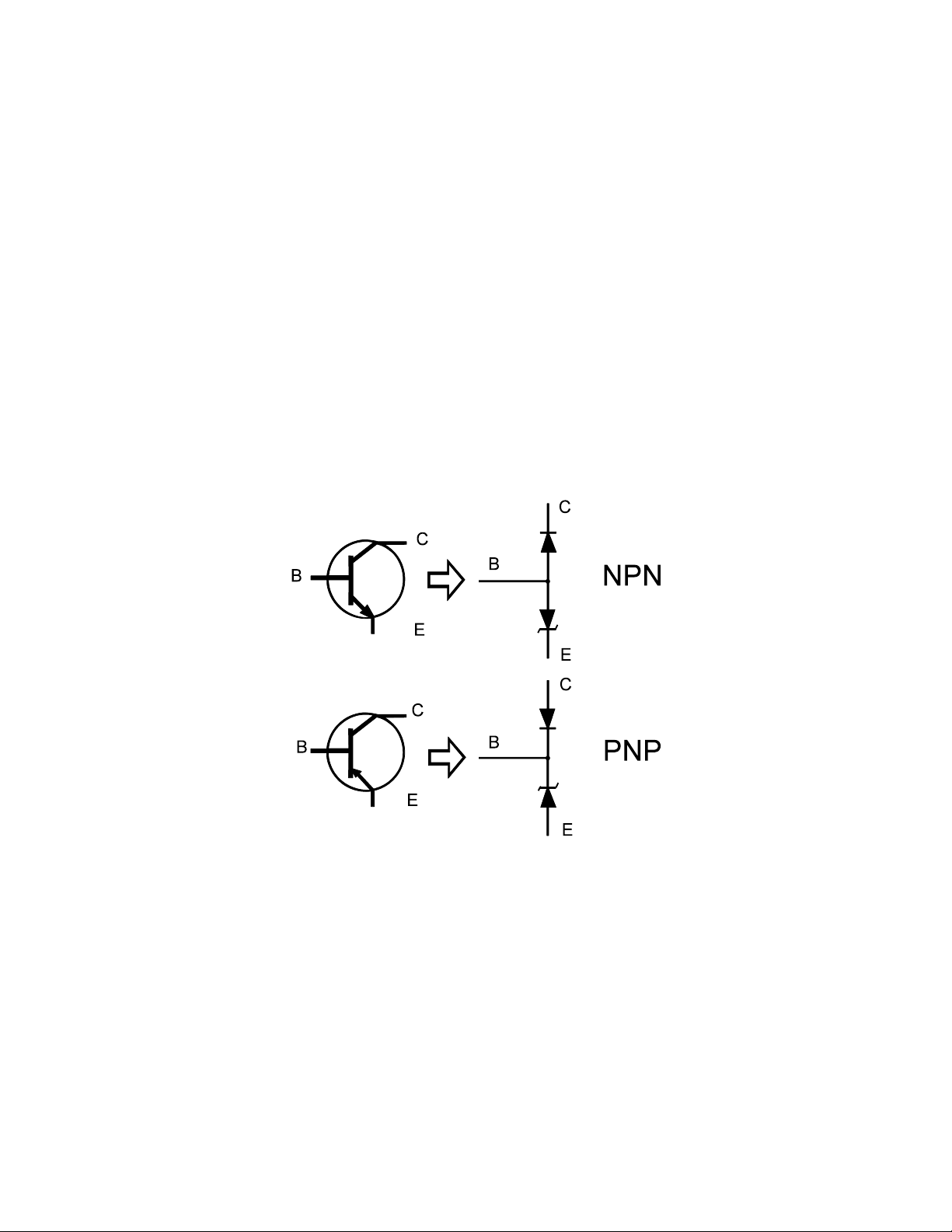
In order to better understand the signatures that transistors create on the Tracker 2800, we can model
these devices in terms of equivalent diode circuits. These are shown in figure 4-19. These figures show
that the collector-based junction analog signature looks similar to a diode signature, and the emitter-
base junction signature looks similar to a zener diode signature. Because we have already seen the
signatures of these two types of junctions when we tested diodes, they should be familiar to you.
Figure 4-19. NPN and PNP Bipolar Transistor Equivalent Circuits
Bipolar Transistor Base-Collector Signatures
Do the following to display the analog signatures of a bipolar transistor:
1. Select the 1K and 15V.
2. Place or clip the red test lead from the Tracker 2800's Channel A jack to collector lead of the
transistor.
3. Place or clip the black test lead from the Tracker 2800's Common jack to base lead of the
transistor.
67
Diode 1N914 PNP 2N3906 NPN PN2222A
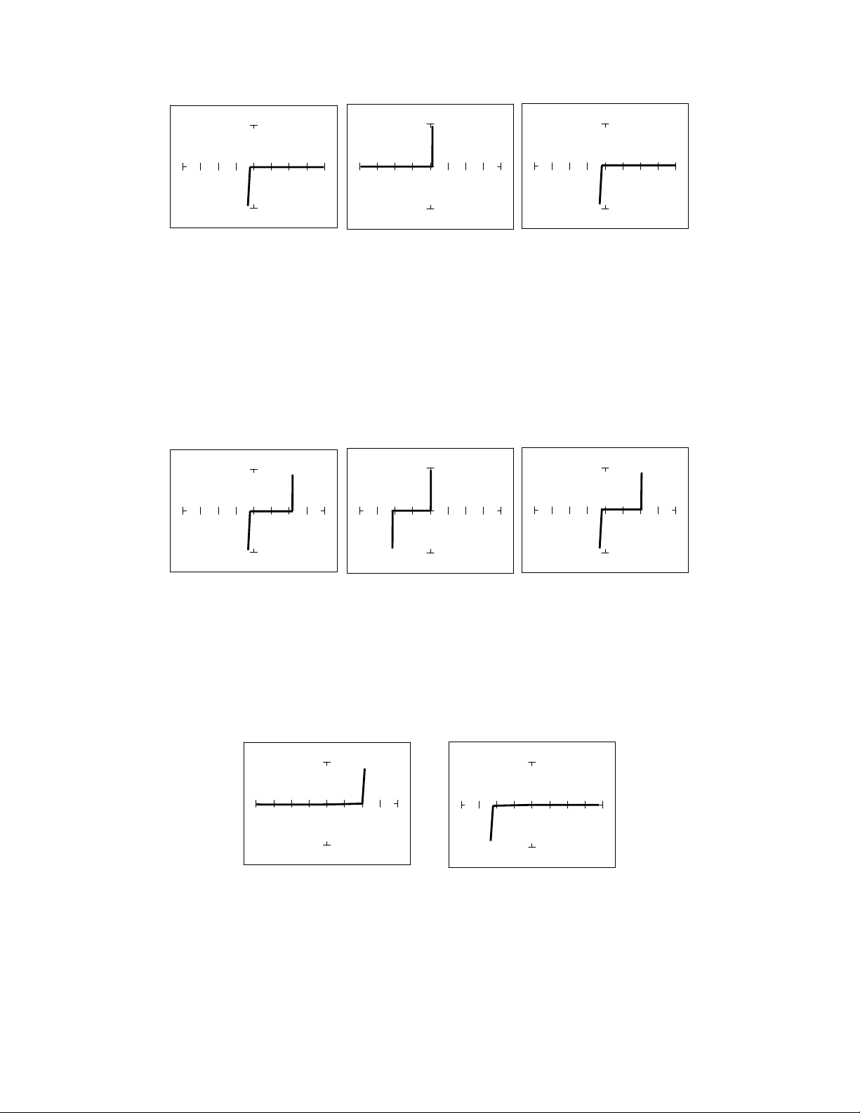
Figure 4-20. Signatures of a Diode and Collector-Base of Transistors at 1K and 15V.
Notice that the collector-base signature of a NPN transistor is identical to the signature of diode. The
collector-base signature of a PNP transistor, which has opposite polarity from a NPN, looks similar to
a diode with its polarity reversed. These are the signatures we expected from our circuit modeling. We
can do the same kind of comparison with the emitter-base circuits.
Zener Diode 1N5239B PNP 2N3906 NPN PN2222A
Figure 4-21. Signatures of a Diode and Emitter-Base of Transistors at 1K and 15V.
We can see that the base-emitter signature of the NPN transistor is nearly identical to the signature of
the zener diode. The emitter-base signature of a PNP transistor is also nearly identical but opposite in
polarity to the zener diode.
PNP Transistor - 2N3906 NPN Transistor - PN2222A
Figure 4-22. Signatures of the Collector-Emitter of Transistors at 1Kand 15V.
You can see that the collector-emitter signature of a PNP transistor looks like a forward biased diode
with the knee at approximately +7 Volts. The collector-emitter signature of a NPN transistor looks
similar to a reverse biased diode with the knee at approximately -7 Volts.