Tracker-2800-2800S.pdf - 第78页
78 CMOS Logic Family CMOS circuits are constructed differentl y than TTL circuits. The inputs to CM OS transistors are capacitive due to the use of field-effect transistors (FET) instead of bipolar t ransistors used in T…
77
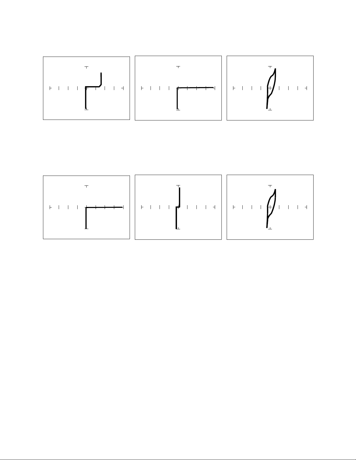
Pin 1 input Pin 2 output Pin 14 power
20V, 10K, 200Hz 20V, 10K, 200Hz 10V, 100, 200Hz
Figure 5-4. Signatures of a 7404 Hex Inverter.
Pin 1 input Pin 2 output Pin 14 power
20V, 10K, 200Hz 20V, 10K, 200Hz 10V, 100 200Hz
Figure 5-5. Signatures of a 74LS04 Hex Inverter.
Note the differences between the two logic families. They have the same logic function but different
construction, therefore different signatures. To test one of these chips without another reference chip
available just compare each input's signature with the other five inputs. Similarly, compare each
output's signature with the other five outputs.
78
CMOS Logic Family
CMOS circuits are constructed differently than TTL circuits. The inputs to CMOS transistors are
capacitive due to the use of field-effect transistors (FET) instead of bipolar transistors used in TTL.
In this example, we will choose a 74HC14 Schmidt
Trigger Hex Inverter. The HC designation means that
it's a member of the high-speed CMOS logic family.
From the block diagram of this part, you can see that it
has only four different circuit functions. They are
inverter input, inverter output, power supply V
CC
input,
and power supply ground.
Do the following to display the analog signatures of a digital IC:
1. Select the 50 and 10V, 60 Hz range.
2. Place or clip the black test lead from the Tracker 2800's Common jack to the IC's ground pin. For
this example, the ground pin of the 74HC14 is pin 7.
3. Use the red test lead from the Tracker 2800's Signal jack and probe each pin of the IC. For this
example, pins 1, 3, 5, 9, 11, and 13 are all input buffer circuits so they will have identical
signatures. (Note: This is only for ICs out of circuit.)
4. Similarly, use the red test lead and probe the output buffer pins 2, 4, 6, 8, 10, and 12. These pins
will have the same signatures. (Note: This is only for ICs out of circuit.)
5. Use the red test lead from the Tracker 2800's Signal jack and probe the power supply V
CC
input
pin. For this example, the V
CC
pin of the 74HC14 is pin 14.
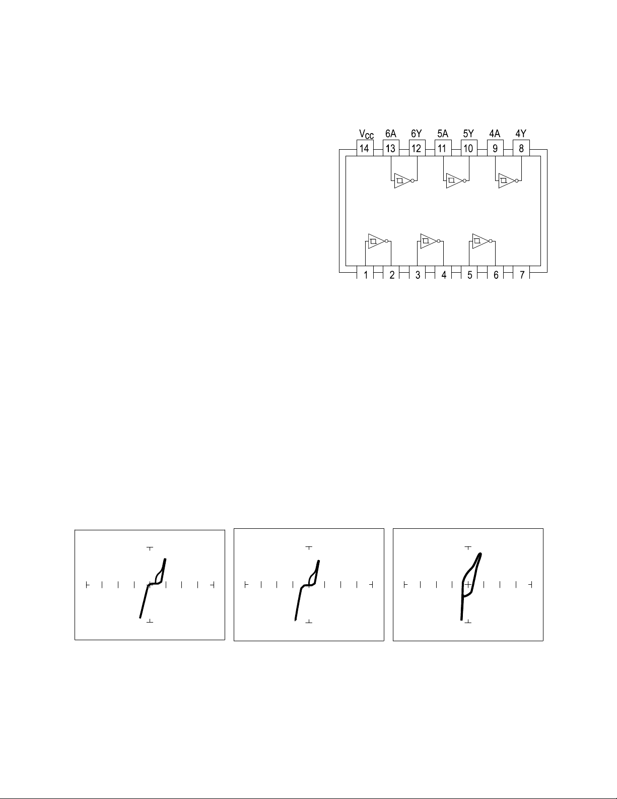
Pin 1 – Input Pin 2- Output Pin 14 - V
CC
Figure 5-7. Signatures of a 74HC14 CMOS Hex Inverter in 50, 10V, 60Hz Range
Figure 5-6. 74HC14 Block Diagram.
79
CMOS Components and Test Signal Frequency - F
S
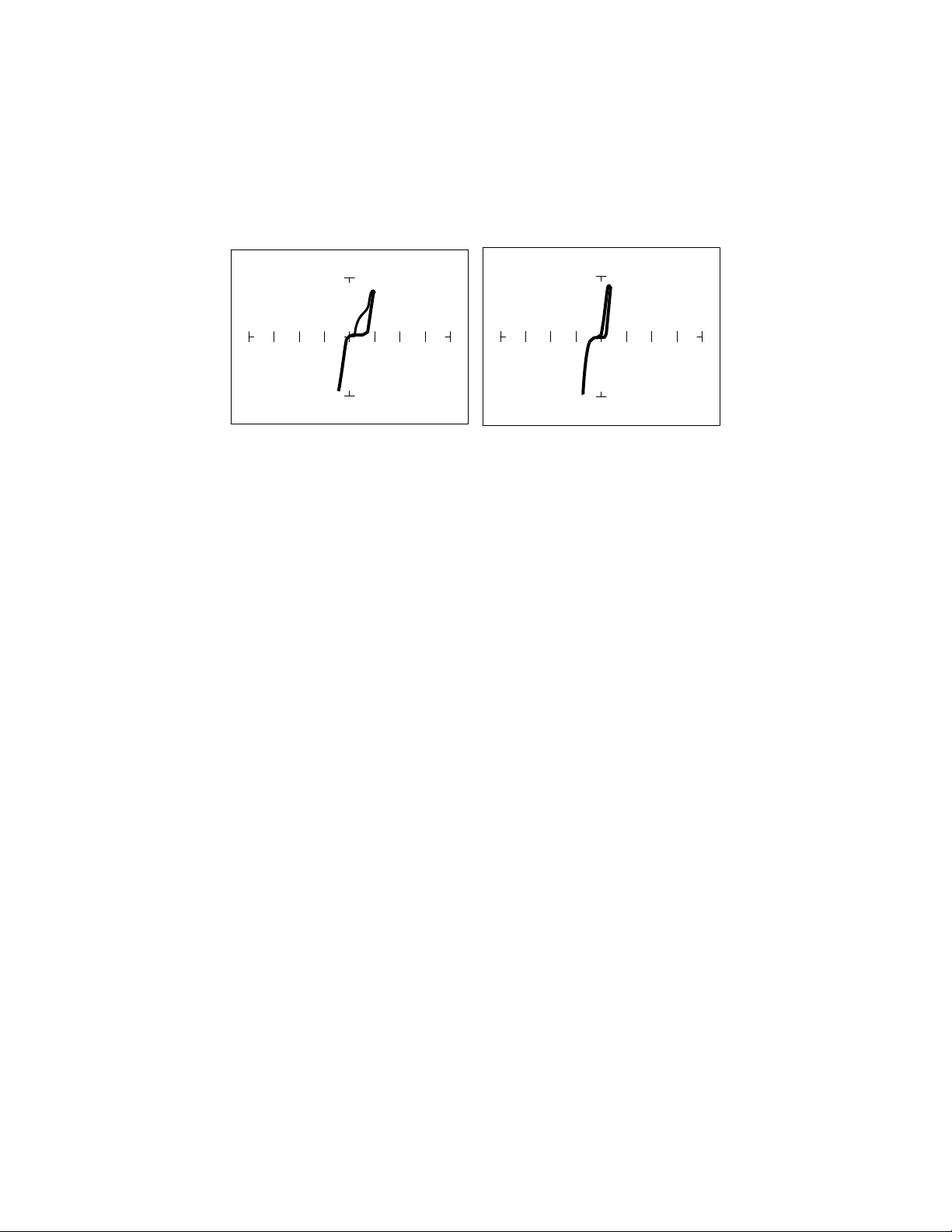
CMOS logic circuits inherently have a significant amount of internal capacitance. This junction
capacitance is visible in the CMOS signatures when using the Tracker 2800. Capacitance in CMOS
circuitry may be emphasized or de-emphasized by changing the frequency of the test signal.
F
S
= 20 Hz F
S
= 400 Hz
Figure 5-8. Signatures of a 74HC14 Input Pin at Different Frequencies in 10V, 1K Range
Troubleshooting Digital Logic ICs
Comparison testing is a very powerful and effective test strategy when troubleshooting digital logic
using ASA. The Tracker 2800's Alt feature makes this technique quick and simple. Instead of having
to remember the specific signatures of a good component, all that's needed is to have a reference
component or board beside the one that's suspect. This section gave many examples of signatures from
TTL, Schottky TTL and CMOS logic families. Although from first inspection, these signatures appear
to be complex, remember that each of the ICs in the examples had really only four unique signatures
(buffer input, buffer output, power supply VCC and power supply ground). We can use this
characteristic to develop an effective model for troubleshooting digital logic chips.
1. Select the 50, 10V and 60 HZ range
2. Place or connect the black or blue ground clip lead from the Tracker 2800's Common jack to both
reference and suspect ICs or the board’s ground pin.
3. Place or clip the red test lead from the Tracker 2800's Channel A test terminal to the reference or
known good IC's pin. For this example, start with pin 1 of the known good IC.
4. Observe the signature. This is the signature of the pin of the known good component.
5. Keep the red probe on pin 1, an input pin. Probe all the other input pins of the suspect component
with the black probe until you have identified all the pins that have signatures that are the same as
pin 1.
6. Move the red probe on pin 2, an output pin. Probe all the other output pins of the suspect
component with the black probe until you have identified all the pins that have signatures that are
the same as pin 2.