Tracker-2800-2800S.pdf - 第75页
75 Digital Integrated Circuit s Before we examine the analog si gnatures of an IC, let's stud y the block diagram of a 74LS245 octal bi- directional bus buffer to introduce some basic concepts. T his IC is a member …

74
SECTION 5 TESTING INTEGRATED CIRCUITS
5-1. DIGITAL INTEGRATED CIRCUITS
Digital integrated circuit (IC) chips are made from transistors on a common substrate. Their analog
signatures are typically variations of the discrete diode and transistor signatures. Most logic ICs,
contain multiple circuits in one chip. These chips can have pins from 14 to over 200, although quite
often many pins share quite similar signatures. This can make troubleshooting easier by giving us an
easy-to-find signature to use as a comparison. In this section, it is important to understand how the
Tracker 2800 and ASA respond to these circuits.
Integrated Circuit Failures
A functioning IC may stop working for a number of reasons. Some of the most common causes of IC
failures are:
EOS - Electrical Over Stress. The IC’s maximum electrical specifications have been exceeded. This
condition may result in the IC developing internal shorts and opens.
ESD - Electrostatic Discharge. Repeated exposure may cause internal resistance to develop in the
IC junctions. This internal resistance may vary from 5 k to 25 k with a typical value of 20 k. ESD
exposure can cause internal flaws such as resistance, opens and shorts.
Dendrites - A process flaw, that results in particles growing between conductors on a substrate
causing shorts.
Ionic - Contamination introduced at the time of manufacturing that contamination develops into
leakage between substrate channels. This causes 5 k to 25 k of resistance.
Purple Plague - Destructive interaction between gold and aluminum metal layers. Junction
connections become very brittle and may cause internal opens.
Corrosion or Electromigration - Another process flaw in which aluminum metallization causes
pinholes, corrosion and resistance. This will create opens and resistance.
75
Digital Integrated Circuits
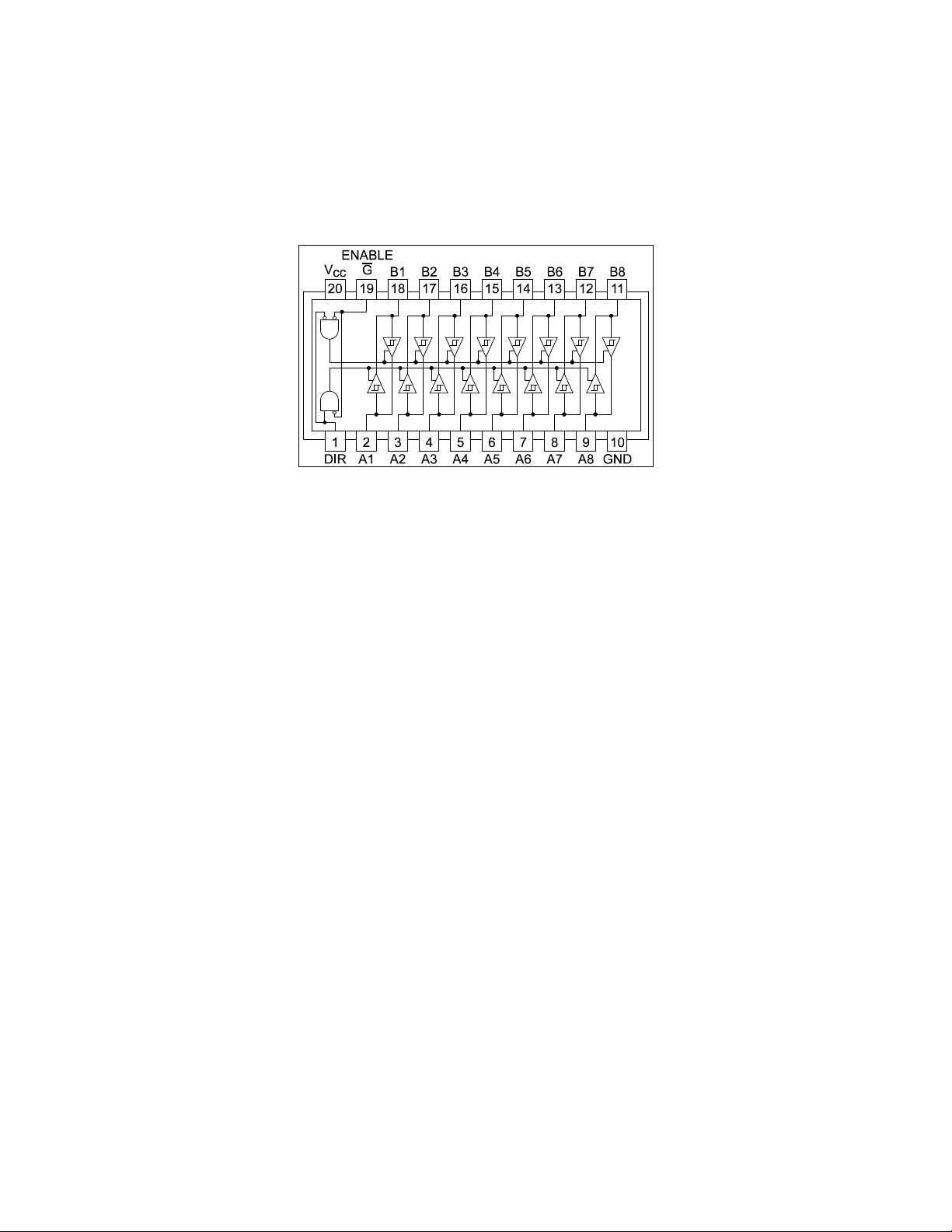
Before we examine the analog signatures of an IC, let's study the block diagram of a 74LS245 octal bi-
directional bus buffer to introduce some basic concepts. This IC is a member of the low power
Schottky transistor-transistor logic family (LSTTL). Examine the block diagram for this chip below.
You will see that there are only four different kinds of circuits on this chip.
Figure 5-1. Digital IC 74LS245 Block Diagram.
Circuit 1 - Pins 2 through 9 and 11 through 18 are all the same function. Each pin is connected to
both an input and an output of a buffer.
Circuit 2 - Pins 1 and 19, although they have different names, are both enables and are inputs to
AND gates.
Circuit 3 - Power supply ground input, pin 10.
Circuit 4 - Power supply V
CC
input, pin 20.
Each circuit type will produce a different analog signature. Because there are only four types of circuits
on the chip, there will be only four unique analog signatures when out of circuit.
Signatures of a Digital IC
Do the following to display the analog signatures of a digital IC (out of circuit):
1. Select the 5V, 10K, 200Hz Range.
2. Place or clip the black test lead from the Tracker 2800's Common jack to the IC's ground pin. For
this example, the ground pin of the 74LS245 is pin 10.
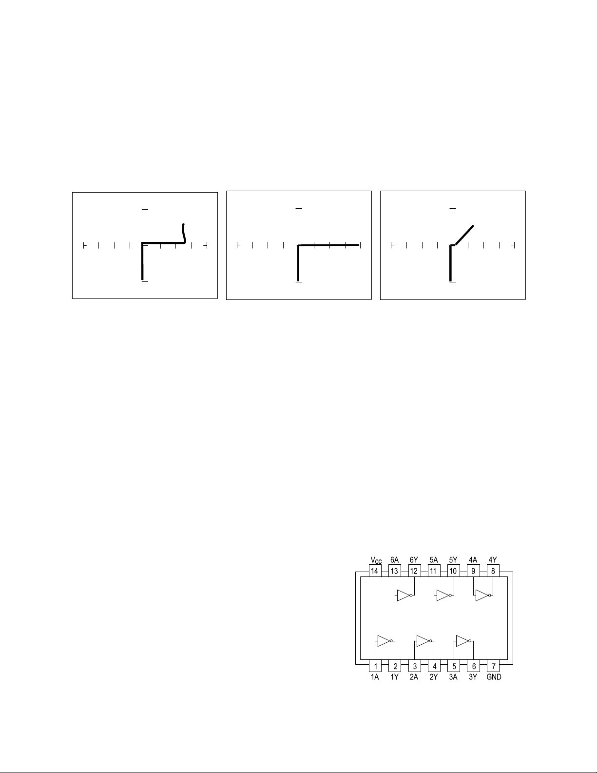
3. Use the red test lead from the Tracker 2800's Channel A jack. Probe each pin of the IC and view its
signature on Tracker 2800's signature display. For this example, pins 2 to 9 and 11 to 18 are all
buffer circuits so they will have identical signatures. (Note: This is only for ICs out of circuit.)
76
4. Use the red test lead from the Tracker 2800's Signal jack. Probe the enable input pins of the IC and
view their signatures on the signature display. For this example, the enable pins of the 74LS245 are
pin 1 and 19 and will have the same signatures. (Note: This is only for ICs out of circuit.)
5. Change the range to 10V, 100, 200Hz. Use the red test lead from the Tracker 2800's Signal jack.
Probe the power supply V
CC
input pin and view its signature on the signature display. For this
example, the V
CC
pin of the 74LS245 is pin 20.
Buffer pins Enable pins V
CC
Power pin
20V, 10K, 200Hz 20V, 10K, 200Hz 10V, 100, 200Hz.
Figure 5-2. Signatures of a Digital IC, 74LS245. Ground Pin to Test Common
Compare these signatures with other signatures of discrete components such as transistors and diodes.
Note that there are quite a few similarities here.
Signatures for Different Logic Chip Families
There are a wide variety of logic circuit families. Each has its special functions, advantages, and
limitations. They range from TTL and its variations (F, LS, S, etc.), emitter-coupled logic (ECL), to
the complementary metal oxide semiconductor (CMOS) and its variations (C, HC, HCT, VC, etc.).
Comparing Two TTL Logic Families
Although the logic function is the same, there are differences in the circuitry of each logic family.
These differences can be readily seen in their signatures
using the Tracker 2800.
We will illustrate these concepts with the following example of
two hex inverters, a 7404 and a 74LS04 from different logic
families. From the logic diagram below, you can see that they
have the same logic functions and pin order. The difference is that
the LS chip uses Schottky transistors in its internal
construction for increased performance and reduced power
consumption. Note that there are only four types of circuit
connections and therefore only four signatures on this
chip: inverter inputs, inverter outputs, V
CC
and ground.
Figure 5-3. Diagram of 7404 & 74LS04.