SIPLACE Line Computer UNIX.pdf - 第238页
8 Product / PCB User M anual Line Computer UNI X 8.1 PCB Editor Software Version 5 02.xx 10 /2000 Issue 236 I t I I 8.1.1 Desc ription of a PCB 8.1.1.1 PCB Data The PCB data can be catego rized into source dat a and proc…

User Manual Line Computer UNIX 8 Product / PCB
Software Version 502.xx 10/2000 Issue 8.1 PCB Editor
235
I
t I I
8 Product / PCB
8.1 PCB Editor
The PCB Editor enables the user to give a hierarchical description (pyramidal structure) of the PCB to be
assembled.
The PCB Editor is subdivided into the following sub-editors:
- Structure Editor
The Structure Editor provides the user with an overview of the overall structure of a PCB. It is
possible to create new PCB types and to edit existing ones.
As an option, the entire PCB including all placement positions, fiducials, ink spots, coordinate
systems, etc. can be represented graphically in the display area of the Structure Editor.
- Cluster Editor
The Cluster Editor serves to define or edit the basic data (cluster data) of a PCB.
- Placement Position Editor
The Placement Position Editor describes the location of the placement positions.
- Fiducial Editor
Fiducials, fiducial sets and ink spots can be defined or edited in the Fiducial Editor.

8 Product / PCB User Manual Line Computer UNIX
8.1 PCB Editor Software Version 502.xx 10/2000 Issue
236
I
t I I
8.1.1 Description of a PCB
8.1.1.1 PCB Data
The PCB data can be categorized into source data and process-specific data.
- The source data contain the description of a PCB.
- The process-specific data are generated from the source data for a given system, i.e. for a given
setup selected by the user.
8.1.1.2 PCB Source Data
- PCB Type
The PCB type contains the basic description of a PCB type consisting of data for clusters, fiducials,
component positions as well as cross-references given to other descriptions of partial PCB structures.
Sample file name of PCB type "A": A.lb
- Partial PCB Structure
This partial PCB structure contains the PCB type description as well as its coordinate data
(see Fig. 8.1.2).
Sample file name of partial PCB structure "A": A.lp
- Overall PCB Structure
When the generated process-specific data are added to the source data, then all data required for
assembling the PCB are available.
Sample file name of overall PCB structure "A": A.la
User Manual Line Computer UNIX 8 Product / PCB
Software Version 502.xx 10/2000 Issue 8.1 PCB Editor
237
I
t I I
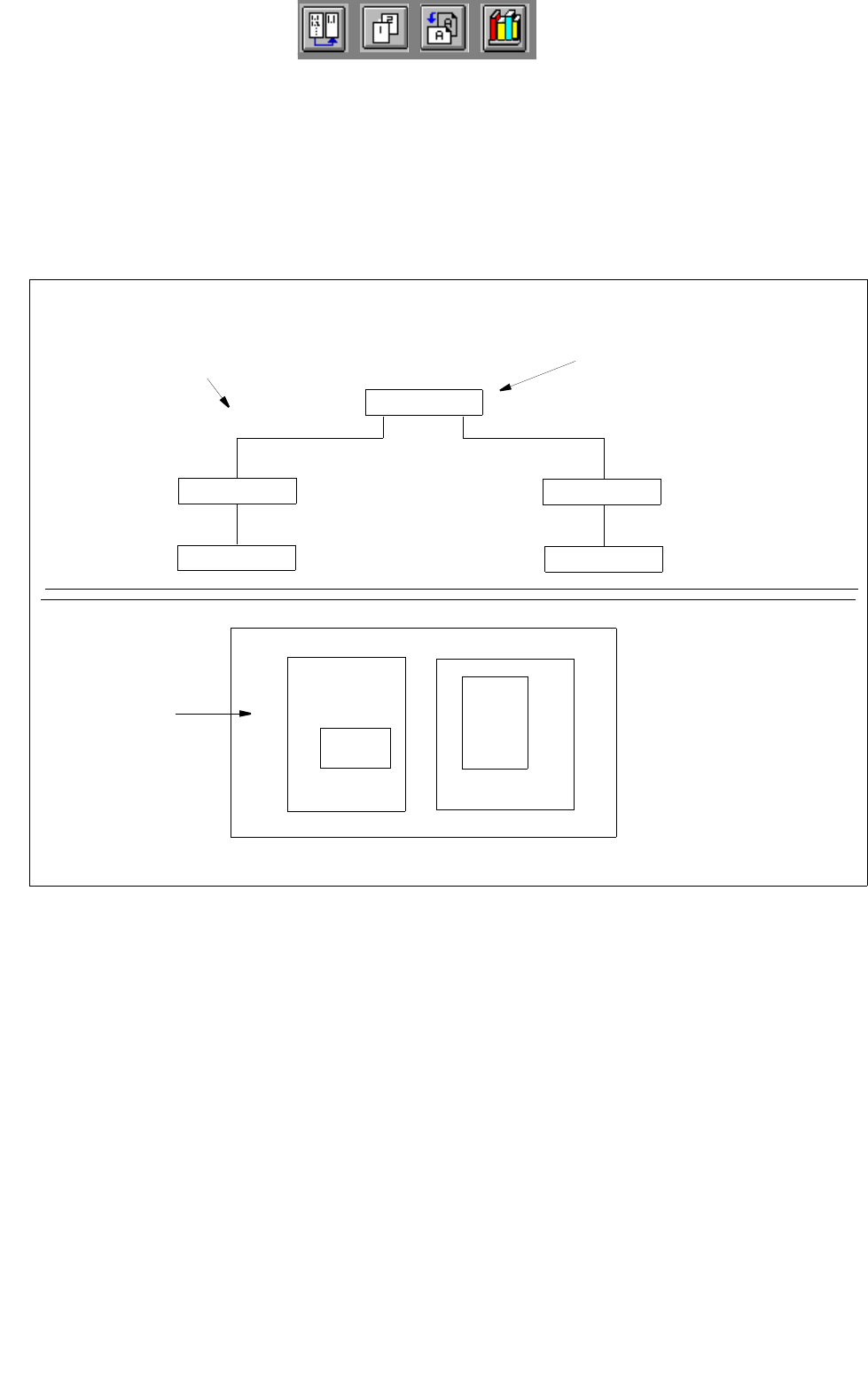
8.1.1.3 PCB Structure
PCBs can be linked (as in a network) to other PCBs via their partial structures. A PCB to be assembled is loaded
into the PCB Editor by entering the name (name.la) of the overall PCB structure.
In the main display window of the PCB Editor, the Structure Editor, the structure of said PCB loaded is displayed
and can be changed. The example in Fig. 8.1.1 shows such a structure and the associated PCB layout.
Fig. 8.1.1 PCB Structure (sample PCB "A")
PCB B
PCB C
LP E
LP D
overall PCB structure
(displayed in the display area)
associated
PCB layout
uppermost partial structure
in the overall PCB structure
PCB B
PCB C
PCB A
PCB
PCB D
PCB D
PCB E
PCB A
PCB B
PCB C