SIPLACE Line Computer UNIX.pdf - 第556页
17 Practical Tips on Using the LC UNIX User Manual Line Computer UNIX 17.3 Description of Com ponents and PC Bs Software Version 5 02.xx 10 /2000 Issue 554 I t I I The pac kage form de scrip tion is dis pensed wi th. The…
User Manual Line Computer UNIX 17 Practical Tips on Using the LC UNIX
Software Version 502.xx 10/2000 Issue 17.3 Description of Components and PCBs
553
I
t I I
pattern_2
pattern_1
pattern_3
pattern_4
board 1
board2
board 3
board 1
board2
board 3
board 3
board2
board 1
board 3
board2
board 1
Example_3
5
10
15
Corner
17.3.3 PCB 3: Focus on Cluster Technique
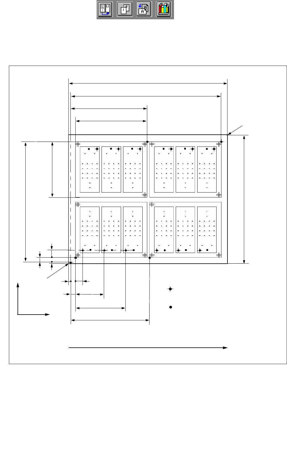
PCB 3 consists of four clusters (pattern) each of which comprises three single circuits (board). The dimensions
and the placement configuration of the single circuits corresponds to those of PCB 2. Clusters 3 and 4 are ro-
tated by 180°. For each cluster a PCB position recognition operation is performed. Three fiducials are available
in each case. An ink spot is located on each single circuit.
335
272
5
X
Y
PCB coordinate
system 0°
Direction of travel
150
116
10
15
60
105
165
Corner
PCB height= 1.5 mm
Zero point of the different levels:
PCB, cluster, single circuit
Ink spot
Fig. 17.3.7 Dimensions PCB 3
252
160
315
17 Practical Tips on Using the LC UNIX User Manual Line Computer UNIX
17.3 Description of Components and PCBs Software Version 502.xx 10/2000 Issue
554
I
t I I
The package form description is dispensed with.
The component description is dispensed with.
The adhesive pattern description is dispensed with.
No fiducials are present.
No ink spot is present.
The placement positions are defined in the
single circuits.
Pack. form description
Starting the PCB
Editor for a PCB
Indicating position of
PCB in the machine
Defining ink spot
Component description
Adh. pattern description
Entering dimensions
of PCB
Defining fiducials
continued on page 17-44
Cluster Editor
Fiducial Editor
Entering placement
positions
PCB description
User Manual Line Computer UNIX 17 Practical Tips on Using the LC UNIX
Software Version 502.xx 10/2000 Issue 17.3 Description of Components and PCBs
555
I
t I I
17.2.3.1 Package form description
PCB 3 consists of four clusters with three single circuits each, all of which correspond to PCB 2.
For the package form description refer to section 17.2.2.1
17.2.3.2 Component description
PCB 3 consists of four clusters with three single circuits each, all of which correspond to PCB 2.
For the component description refer to section 17.2.2.2
17.2.3.3 Adhesive pattern description
PCB 3 consists of four clusters with three single circuits each, all of which correspond to PCB 2.
For the adhesive pattern description refer to section 17.2.2.3.
17.2.3.4 PCB description
The offset values are to be determined automatically from Fig. 17.3.7 on page 17-553 (solution on page 17-
563).
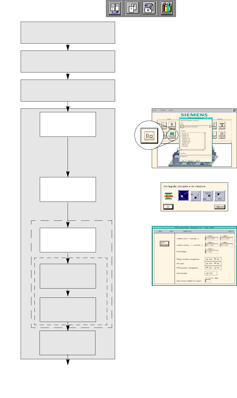
To open the PCB Editor for a PCB, proceed as follows:
1. On the desktop click on the icon the PCB Editor .
The file selection window is opened.
2. Click on the Selection editing field.
3. Enter the name of the PCB, here: Example_3.la, and click on the OK button.
A dialog box is opened.
4. Click on the TYPE editing field.
5. Enter a type designation, here: Typ_1, and click on the OK button:
The Component Editor is opened. The PCB is displayed as a rectangle.
To specify the position of the PCB in the machine:
6. Activate the Coordinate system icon .
7. Click on the PCB (rectangle).
A dialog box containing the display of four coordinate systems is opened.
8. Click on a coordinate system, here: 0°.
9. Click on the OK button.
The dialog box is closed.
To enter the dimensions of the PCB, proceed as follows:
10. Activate the Select icon .
11. Click on the PCB (rectangle).
The rectangle is highlighted in green.
12. Click on the Cluster Editor... option on the SERVICES menu.
The Cluster Editor is opened.
13. Enter the dimensions of the PCB, see Fig. 17.3.7 on page 17-553.
14. Click on the Quit option on the FILE menu.
The Cluster Editor is closed.
Defining fiducials: no fiducials are present.
Defining ink spot: no ink spot is present.
Entering placement positions: the placement positions are defined at a later point in the single circuits.