IPC-7351-2005_表面贴装焊盘布局设计和标准通用要求.pdf - 第15页
www.bzfxw.com Static Charge – An electrical charge that has accumulated or built up on the surface of a material Static Electricity Control – A technique where materials and systems are employed to eliminate/discharge st…

www.bzfxw.com
*Constraining Core – A supporting plane that is internal to
a packaging and interconnecting structure.
Courtyard – The smallest rectangular area that provides a
minimum electrical and mechanical clearance (courtyard
excess) around the combined component body and land
pattern boundaries.
Courtyard Excess – The area between the rectangle cir-
cumscribing the land pattern and the component, and the
outer boundary of the courtyard. The courtyard excess may
be different in the x- and y-direction.
Courtyard Manufacturing Zone – The area that provides
a minimum electrical and mechanical clearance (courtyard
excess) around the combined component body and land
pattern boundries.
*Dual-Inline Package (DIP) – A basically-rectangular
component package that has a row of leads extending from
each of the longer sides of its body that are formed at right
angles to a plane that is parallel to the base of its body.
*Fine-Pitch Technology (FPT) – A surface-mount assem-
bly technology with component terminations on less than
0.625 mm [0.025 in] centers.
*Fiducial (Mark) – A printed board artwork feature(s) that
is created in the same process as the conductive pattern and
that provides a common measurable point for component
mounting with respect to a land pattern or land patterns.
*Flat Pack – A rectangular component package that has a
row of leads extending from each of the longer sides of its
body that are parallel to the base of its body.
*Footprint – See ‘‘Land Pattern.’’
*Grid – An orthogonal network of two sets of parallel
equidistant lines that is used for locating points on a
printed board.
*Integrated Circuit (IC) – A combination of inseparable
associated circuit elements that are formed in place and
interconnected on or within a single base material to per-
form a particular electrical function.
*Jumper wire – A discrete electrical connection that is part
of the original design and is used to bridge portions of the
basic conductive pattern formed on a printed board.
*Land – A portion of a conductive pattern usually used for
the connection and/or attachment of components.
*Land Pattern – A combination of lands that is used for
the mounting, interconnection and testing of a particular
component.
*Leadless Chip Carrier – A chip carrier whose external
connections consist of metallized terminations that are an
integral part of the component body. (See also ‘‘Leaded
Chip Carrier.’’)
Leaded Chip Carrier – A chip carrier whose external con-
nections consist of leads that are around and down the side
of the package. (See also ‘‘Leadless Chip Carrier.’’)
*Master Drawing – A control document that shows the
dimensional limits or grid locations that are applicable to
any and all parts of a product to be fabricated, including
the arrangement of conductors and nonconductive patterns
or elements; the size, type, and location of holes; and all
other necessary information.
Mixed Component-Mounting Technology – A component
mounting technology that uses both through-hole and
surface-mounting technologies on the same packaging and
interconnecting structure.
*Module – A separable unit in a packaging scheme.
Nominal Dimension – A dimension that is between the
maximum and minimum size of a feature. (The tolerance
on a nominal dimension gives the limits of variation of a
feature size.)
*Packaging and Interconnecting Structure (P&IS) – The
general term for a completely processed combination of
base materials, supporting planes or constraining cores, and
interconnection wiring that are used for the purpose of
mounting and interconnecting components.
*Plated-Through Hole (PTH) – A hole with plating on its
walls that makes an electrical connection between conduc-
tive patterns on internal layers, external layer, or both, of a
printed board.
*Primary Side – The side of a packaging and interconnect-
ing structure that is so defined on the master drawing. (It is
usually the side that contains the most complex or the most
number of components.)
*Printed Board (PB) – The general term for completely
processed printed circuit and printed wiring configurations.
(This includes single-sided, double-sided and multilayer
boards with rigid, flexible, and rigid-flex base materials.)
*Printed Wiring – A conductive pattern that provides
point-to-point connections but not printed components in a
predetermined arrangement on a common base. (See also
‘‘Printed Circuit.’’)
*Registration – The degree of conformity of the position
of a pattern (or portion thereof), a hole, or other feature to
its intended position on a product.
*Secondary Side – That side of a packaging and intercon-
necting structure that is opposite the primary side. (It is the
same as the ‘‘solder side’’ on through-hole mounting tech-
nology.)
*Single-Inline Package (SIP) – A component package
with one straight row of pins or wire leads.
IPC-7351 February 2005
4
标准分享网 www.bzfxw.com 免费下载

www.bzfxw.com
Static Charge – An electrical charge that has accumulated
or built up on the surface of a material
Static Electricity Control – A technique where materials
and systems are employed to eliminate/discharge static
electricity build-up by providing continuous discharge
paths
*Supported Hole – A hole in a printed board that has its
inside surfaces plated or otherwise reinforced.
*Supporting Plane – A planar structure that is a part of a
packaging and interconnecting structure in order to provide
mechanical support, thermo-mechanical constraint, thermal
conduction and/or electrical characteristics. (It may be
either internal or external to the packaging and intercon-
necting structure.) (See also ‘‘Constraining Core.’’)
*Surface Mount Technology (SMT) – The electrical con-
nection of components to the surface of a conductive pat-
tern that does not utilize component holes.
*Tented Via (Type I Via) – A via with a mask material
(typically dry film) applied bridging over the via wherein
no additional materials are in the hole. It may be applied to
one side or both.
*Thermal Mismatch – The absolute difference between the
thermal expansion of two components or materials. (See
also ‘‘Coefficient of Thermal Expansion (CTE).’’)
*Through Connection – The electrical connection to con-
nect conductor patterns on the front side through to the
back side of a printed board. (See also ‘‘Interfacial Connec-
tion.’’)
*Through-Hole Technology (THT) – The electrical con-
nection of components to a conductive pattern by the use
of component holes.
*Tooling Feature – A physical feature that is used exclu-
sively to position a printed board or panel during a fabrica-
tion, assembly or testing process. (See also ‘‘Locating
Edge,’’ ‘‘Locating Edge Marker,’’ ‘‘Locating Notch,’’
‘‘Locating Slot,’’ and ‘‘Tooling Hole.’’)
*Via – A plated-through hole that is used as an interlayer
connection, but in which there is no intention to insert a
component lead or other reinforcing material. (See also
‘‘Blind Via’’ and ‘‘Buried Via.’’)
2 APPLICABLE DOCUMENTS
2.1 IPC
1
IPC-A-48 Surface Mount Land Pattern Artwork (Mantech)
IPC-A-49 Surface Mount Land Pattern Artwork (IPC-SM-
782)
IPC-T-50 Terms and Definitions for Interconnecting and
Packaging Electronic Circuits
IPC-A-610 Acceptability of Printed Board Assemblies
IPC-SM-785 Guidelines for Accelerated Reliability Testing
of Surface Mount Solder Attachments
IPC-S-816 SMT Process Guideline and Checklist
IPC-1902 Grid System for Printed Circuits
IPC-2221 Generic Standard on Printed Board Design
IPC-2226 Sectional Design Standard for High Density
Interconnect (HDI) Printed Boards
IPC-2581 Generic Requirements for Printed Board Assem-
bly Products Manufacturing Description Data and Transfer
Methodology
IPC-6012 Qualification and Performance Standard for
Rigid Printed Boards
IPC-7095 Design and Assembly Process Implementation
for BGAs
IPC-7525 Stencil Design Guidelines
IPC-7530 Guidelines for Temperature Profiling for Mass
Soldering Processes
IPC-7711/21 Rework and Repair Guide
IPC-9701 Performance Test Methods and Qualification
Requirements for Surface Mount Solder Attachments
2.2 Electronic Industries Association
2
EIA-481 Tape and Reel Specification
2.3 Joint Industry Standards (IPC)
3
J-STD-001 Requirements for Soldered Electrical and Elec-
tronic Assemblies
J-STD-002 Solderability Tests for Component Leads, Ter-
minations, Lugs, Terminals and Wires
J-STD-003 Solderability Tests for Printed Boards
J-STD-033 Handling, Packing, Shipping and Use of
Moisture/Reflow Sensitive Surface Mount Devices
1. www.ipc.org
2. www.eia.org
3. www.ipc.org
February 2005 IPC-7351
5
www.bzfxw.com
2.4 International Electrotechnical Commission
4
IEC-61188 Printed Boards and Printed Board Assemblies -
Design and Use
2.5 Joint Electron Device Engineering Council (JEDEC)
5
Publication 95 JEDEC Registered and Standard Outlines
for Solid State Products
3 DESIGN REQUIREMENTS
3.1 Dimensioning Systems
This section describes a set
of dimensional criteria for components, land patterns, posi-
tional accuracy of the component placement capability and
the opportunity to create a certain size solder joint com-
mensurate with reliability or product performance analysis.
Profile tolerances are used in the dimensioning system to
define the size range between maximum and minimum
component/lead dimensions without ambiguity. The profile
tolerance is intended to control both size and position of
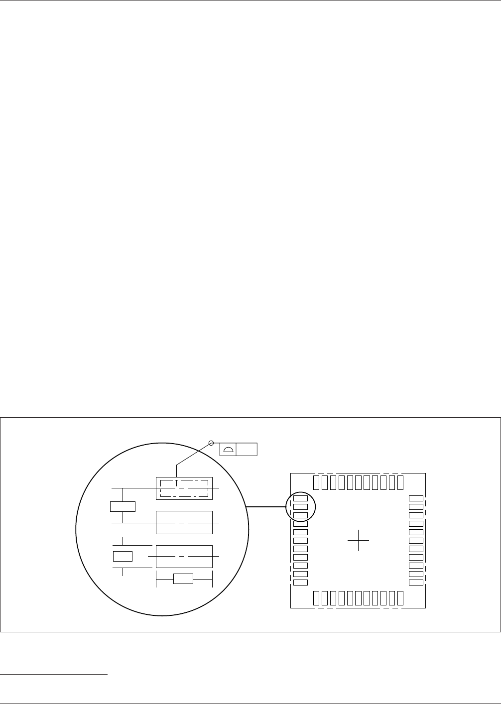
the land. Figure 3-1 shows the profile tolerancing method.
The use of the profile dimensioning system requires an
understanding of the concepts. The use of a set of require-
ments are adopted and invoke the following rules, unless
otherwise modified.
a. All dimensions are basic (nominal).
b. Limits of size control form as well as size.
c. Perfect form is required at maximum dimensions.
d. Datum references and position tolerances apply at maxi-
mum dimensions, and are dependent on feature size.
e. Position dimensions originate from maximum dimen-
sions.
f. Tolerances and their datum references other than size
and position apply regardless of feature size (RFS).
The dimensioning concepts used for this system of analy-
sis consider the assembly/attachment requirements as their
major goal. Specification (data) sheets for components or
dimensions for land patterns on boards may use different
dimensioning concepts, however, the goal is to combine all
concepts into a single system. Users are encouraged to
establish the appropriate relationship between their dimen-
sioning system(s) and the profile dimensioning system and
analysis concepts described herein to allow for ease of tai-
loring these concepts for robust process performance. As
an example, if the tolerance used for positioning is larger
than the machine tolerance used in production, a single
dimensional change could modify the land pattern.
3.1.1 Component Tolerancing The component manu-
facturers and industry standards organizations are respon-
sible for the dimensioning and tolerancing of electronic
components (see 3.1.5.2). The basic dimensions and toler-
ance limits published in the specifications have been con-
verted to a functional equivalent using the profile toleranc-
ing method with all components shown with their basic
dimensions as limit dimensions (maximum or minimum
size). Profile tolerances are unilateral, and are described to
reflect the best condition for solder joint formation.
The concept for component dimension evaluations is based
on evaluating the surfaces of the component termination
and component lead or contact that are involved in the
4. www.iec.ch
5. www.jedec.org
IPC-7351-3-01
Figure 3-1 Profile Tolerancing Method
0.7
1.27
▼
▼
▼
▼
▼
2.5
MMC
▼
▼
▼
0.1
MMC
"
N
"
Places
IPC-7351 February 2005
6
标准分享网 www.bzfxw.com 免费下载