IPC-7351-2005_表面贴装焊盘布局设计和标准通用要求.pdf - 第82页
The land patterns are shown in documentation designed to provide a clear view of the soldering characteristic in such a way that land geometry is visible, and solder joint evalu- ation can be achieved. The same in-proces…
Appendix A
(Informative)
Test Patterns – Process Evaluations
The following test patterns have been developed as stan-
dards that may be used for the evaluation of standard board
materials, with a variety of standard parts. IPC-A-49 art-
work is available for these tests. The land patterns repre-
sent land pattern designs from the original IPC-SM-782
land pattern standard.
The test specimen contains conductors and plated-through
holes and parts connected in a single daisy chain. One end
of the daisy chain is connected to a common ground while
the other end of the chain is connected to land patterns,
then to a plated-through hole in which a wire may be sol-
dered for test purposes.
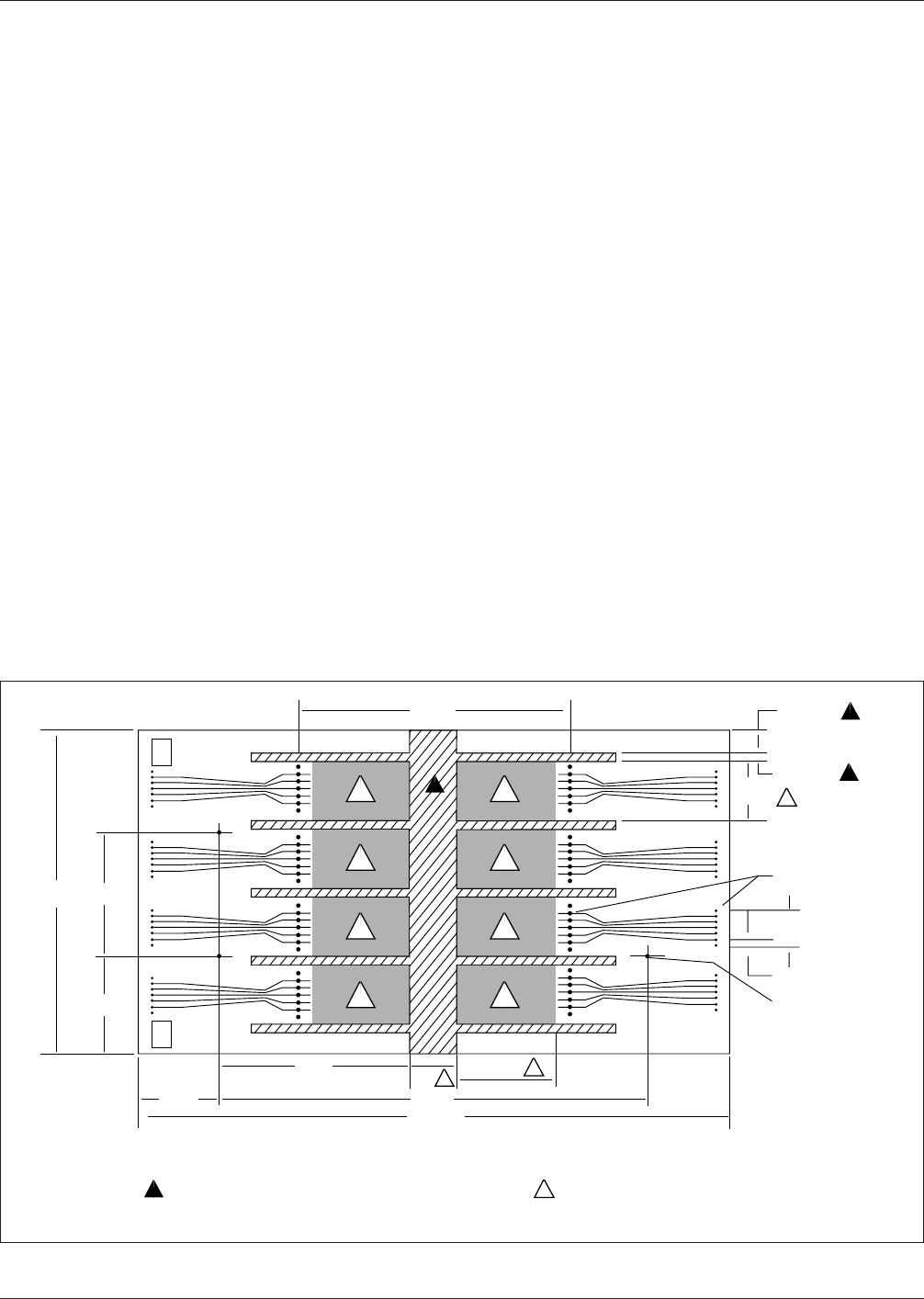
Circuits that are shown in Figure A-1 and Figure A-2 con-
tain the various components listed:
A.1 Test Vehicle Another test specimen is used for the
testing of printed board structures that are intended to pro-
vide P&I structures used primarily for the mounting of
leadless chip carriers. This test board is described in sur-
face mount Air Force Mantech artwork (IPC-A-48). The
board is a 12-layer multilayer board which contains 38
positions for mounting leadless chip carriers used by a sur-
face mount evaluation program to evaluate printed board
and substrate materials. The test boards produced from this
artwork may contain metal cores, or other planes that con-
trol the coefficient of thermal expansion of the P&I struc-
ture.
The following are some examples of the type of materials
that may be used as the constraining core.
a) Nonorganic materials (alumina)
b) Porcelainized clad invar materials
c) Printed boards bonded to low-expansion support (metal
or nonmetal)
d) Compliant layer constructions
e) Metal core boards
A.2 Test Patterns - In-Process Validator Test patterns
to validate in-process conditions are encouraged to be
incorporated into the panel of a printed board assembly.
These designed-in land patterns provide special features for
automatic optical inspection and visual inspection.
IPC-7351-a-01
Figure A-1 General Description of Process Validation Contact Pattern and Interconnect
5
5
5
5
5
5
5
5
+ 41023 -
+ 1 2 -
4 0 3
+ 41023 -
+ 1 2 -
4 0 3
+ 41023 -
+ 1 2 -
4 0 3
+ 41023 -
+ 1 2 -
4 0 3
+ 14032 -
+ 4 3 -
1 0 2
+ 14032 -
+ 4 3 -
1 0 2
+ 14032 -
+ 4 3 -
1 0 2
+ 14032 -
+ 4 3 -
1 0 2
5.600
▼
▼
▼
▼
I.D.I.D.
2.500
▼
▼
2.125
6.745
▼
▼
1.000
4.010
REF
▼
▼
1.490
▼
▼
4
REF
9.020
▼
▼
4
12 ± 1/32
▼
▼
Note: 1. Board G-10 thickness 0.040 - 0.036 2. Primary (top) side
3. Secondary (bottom) side, left-right mirror image
No pattern or components in those
indicated areas allowed 8 sites for test components
5
0.505 REF
▼
▼
▼
▼
▼
▼
▼
▼
▼
▼
▼
0.140 TYP
1.260
TYP REF
4
5
4
0.035 ± 0.003 DIA,
96 HOLES, PTH
0.600 ± 0.003 TYP
0.100 ± 0.003 TYP
0.125 DIA,
3 HOLES
12
3
4
56 7
8
4
2.000 REF
5
▼
▼
▼
▼
▼
All dimensions are in inches
February 2005 IPC-7351
71
The land patterns are shown in documentation designed to
provide a clear view of the soldering characteristic in such
a way that land geometry is visible, and solder joint evalu-
ation can be achieved. The same in-process validator is
used to check the registration of solder paste prior to reflow
soldering.
IPC/EIA J-STD-001 provides the key variables for meeting
soldering requirements that are necessary for various sur-
face mount parts. Land pattern samples provided around
the periphery of a panel, should be designed to provide
clear visibility of the solder joints shown in these figures.
A.3 Stress Testing Stress testing usually consists of
temperature cycling of the printed board assembly that has
been surface mounted through various extremes. The tem-
perature cycling of the assembly or a coupon may be vari-
ety of cycling exposure (see Table 3-16).
During the cycling processes, daisy-chained plated-through
holes and daisy-chained solder joints are measured during
the initial phase as to their resistance, and then monitored
for increased resistance during the thermal cycling. See
IPC-SM-785 and IPC-9701 for additional information.
IPC-7351-a-02
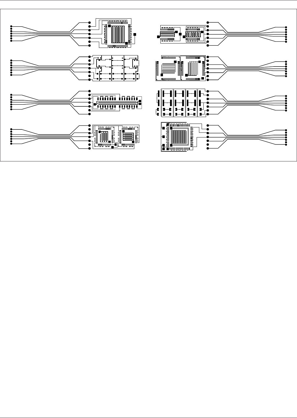
Figure A-2 Photoimage of IPC-A-49 Test Board for Primary Side
IPC-7351 February 2005
72
标准分享网 www.bzfxw.com 免费下载

Appendix B
(Informative)
Abbreviations and Definitions
ATE Automated Test Equipment
COB Chip-on-Board
CTE Coefficient of Thermal Expansion
DIP Dual-in-Line Package
DTP Diameter of True Position
FTP Fine Pitch Technology
IC Integrated Circuit
ICT In-Circuit Test
IR Infrared
LMC Least Material Condition
MMC Maximum Material Condition
OA Organic Acid
OSP Organic Solderability Protection
PB Printed Board
PTFE Polytetrafluoroethylene
PTH Plated-through Hole
RA Rosin Activated
RFS Regardless of Feature Size
RMA Resin Mildly Activated
RMS Root Mean Square
SA Synthetic-Activated
SFA Standard Fabric Allowances
SIP Single In-Line Package
SMA Synthetic Mildly Activated
SMOBC Solder Mask Over Bare Copper
SMT Surface Mount Technology
SOIC Small Outline Integrated Circuit
THT Through-Hole Technology
February 2005 IPC-7351
73