IPC-7351-2005_表面贴装焊盘布局设计和标准通用要求.pdf - 第58页
order to provide an adequate heat transfer path, there is no clearance between the body of the component and the packaging and interconnect structure. This design may accommodate the reflow or wave soldering processes. 8.…
8.5 Metal Electrode Face Diodes (DIOMELF, RES-
MELF)
Resistors, ceramic capacitors, and tantalum
capacitors may all be packaged in these tubular shapes.
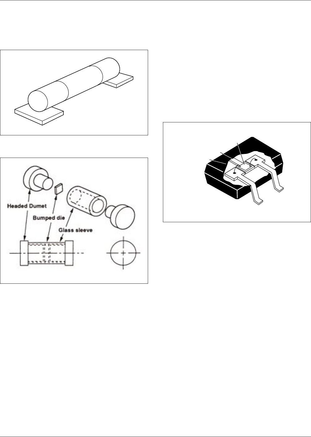
8.5.1 Basic Construction See Figures 8-6 and 8-7.
8.5.2 Marking Parts are available with or without
marked values.
8.5.3 Carrier Package Format Bulk rods, 8 mm tape/4
mm pitch is preferred for best handling. Tape and reel
specifications provide additional requirements.
8.5.4 Resistance to Soldering Parts should be capable
of withstanding five cycles through a standard reflow sys-
tem operating at 215 °C [419 °F]. Each cycle shall consist
of 60 seconds exposure at 215 °C [419 °F]. Parts must also
be capable of withstanding a minimum of 10 seconds
immersion in molten solder at 260 °C [500 °F]. See IPC/
JEDEC J-STD-020 for appropriate reflow cycles and pro-
files when using lead free solders.
8.6 SOT23 One of the first active devices in packaged
form for surface mounting was the SOT device. Plastic
encapsulated three terminal devices with leads formed out
from the body were surface mounted to overcome some of
the problems and difficulties in handling dip transistors. In
general, SOT packages are used with diodes, transistors,
and small I/O devices. The SOT 23 package is the most
common three-lead surface mount configuration.
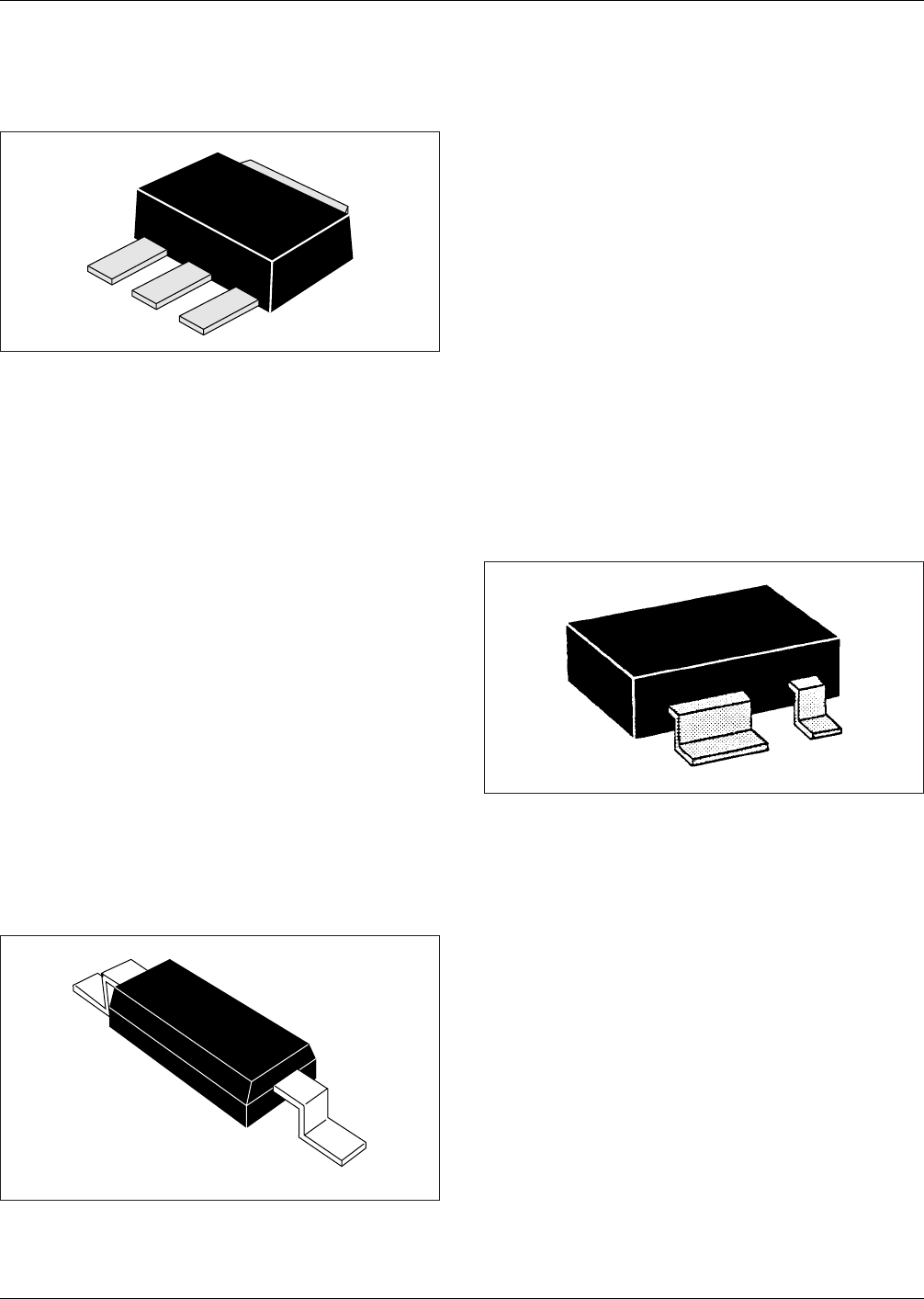
8.6.1 Basic Construction The SOT 23 package has had
several redesigns to meet the needs of both hybrid and
printed board surface mount industries. These changes
resulted in low, medium and high profile characteristics
which basically reflect the clearance that the body is from
the mounting surface. See Figure 8-8 for construction char-
acteristics.
8.6.2 Marking Parts are available with or without
marked values.
8.6.3 Carrier Package Format Carrier package format
shall be according to the following: body type TO-236,
8 mm tape/4 mm pitch.
8.6.4 Resistance to Soldering Parts should be capable
of withstanding five cycles through a standard reflow sys-
tem operating at 215 °C [419 °F]. Each cycle shall consist
of 60 seconds exposure at 215 °C [419 °F]. Parts must also
be capable of withstanding a minimum of 10 seconds
immersion in molten solder at 260 °C [500 °F]. See IPC/
JEDEC J-STD-020 for appropriate reflow cycles and pro-
files when using lead free solders.
8.7 SOT89 These parts are for high power transistors and
diodes. These parts are used where heat transfer to a sup-
porting structure is important. IPC-7352 SOT89 component
outlines are derived from outline TO-243 Issue ‘‘C’’ within
JEDEC Publication 95.
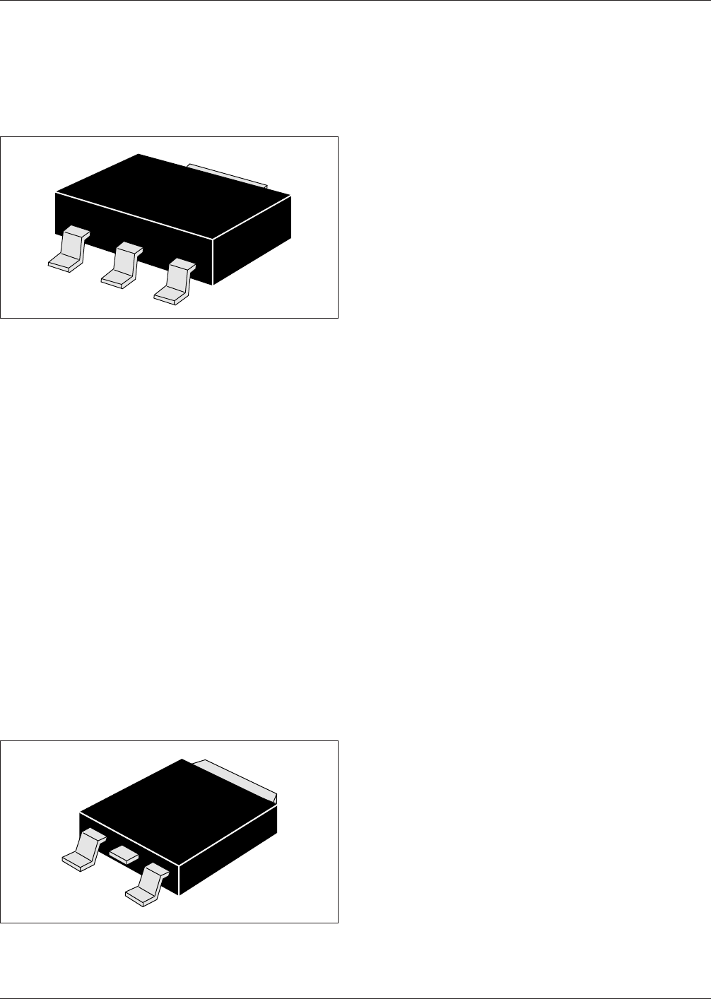
8.7.1 Basic Construction See Figure 8-9. The SOT 89
package dimensions are designed to meet the needs of both
the hybrid and printed board surface mount industries. In
IPC-7351-8-06
Figure 8-6 Metal Electrode Face Component
Construction
IPC-7351-8-07
Figure 8-7 Break-Away Diagram of MELF Components
IPC-7351-8-08
Figure 8-8 SOT 23 Construction
Passivated
Semiconductor Chip
Collector Lead
Bonding Wire
Epoxy Body
Emitter
Lead
Base
Lead
February 2005 IPC-7351
47
order to provide an adequate heat transfer path, there is no
clearance between the body of the component and the
packaging and interconnect structure. This design may
accommodate the reflow or wave soldering processes.
8.7.2 Marking Parts are available with or without
marked values.
8.7.3 Carrier Package Format Carrier package format
shall be according to the following: body type TO-243,
12 mm tape/8 mm pitch.
8.7.4 Resistance to Soldering Parts should be capable
of withstanding ten cycles through a standard reflow sys-
tem operating at 215 °C [419 °F]. Each cycle shall consist
of 60 seconds exposure at 215 °C [419 °F]. Parts must also
be capable of withstanding a minimum of 10 seconds
immersion in molten solder at 260 °C [500 °F]. See IPC/
JEDEC J-STD-020 for appropriate reflow cycles and pro-
files when using lead free solders.
8.8 SOD123 IPC-7352 SOD123 component outlines are
derived from outline DO-214 ‘‘Issue B’’ within JEDEC
Publication 95.
8.8.1 Basic Construction The small outline diode comes
in two configurations. One is a gullwing-leaded (SOD123)
configuration as shown in Figure 8-10. The other is a
molded configuration with terminations (DIOSMB).
8.8.2 Marking Parts are available with or without
marked values.
8.8.3 Carrier Package Format Carrier package formats
are tape and reel; 12 mm tape/8 mm pitch.
8.8.4 Resistance to Soldering Parts should be capable
of withstanding 10 cycles through a standard reflow system
operating at 215 °C [419 °F]. Each cycle shall consist of 60
seconds exposure at 215 °C [419 °F]. Parts must also be
capable of withstanding a minimum of 10 seconds immer-
sion in molten solder at 260 °C [500 °F]. See IPC/JEDEC
J-STD-020 for appropriate reflow cycles and profiles when
using lead free solders.
8.9 SOT143 These parts are for dual diodes and Darling-
ton transistors. IPC-7352 SOT143 component outlines are
derived from outline TO-253 ‘‘Issue C’’ within JEDEC
Publication 95.
8.9.1 Basic Construction The dimensional characteris-
tics are designed to meet the needs of the surface mount
industry. The clearance between the body of the component
and the packaging and interconnect structure is specified at
0.05 mm to 0.13 mm [0.002 in to 0.005 in] to accommo-
date reflow or wave soldering processes (see Figure 8-11).
8.9.2 Marking Parts are available with or without
marked values.
8.9.3 Carrier Package Format Carrier package format
shall be according to the following: body type TO-253,
8 mm tape/4 mm pitch.
8.9.4 Resistance to Soldering Parts should be capable
of withstanding five cycles through a standard reflow sys-
tem operating at 215 °C [419 °F]. Each cycle shall consist
of 60 seconds exposure at 215 °C [419 °F]. Parts must also
be capable of withstanding a minimum of 10 seconds
immersion in molten solder at 260 °C [500 °F]. See IPC/
JEDEC J-STD-020 for appropriate reflow cycles and pro-
files when using lead free solders.
8.10 SOT223 These parts are for dual diodes and Dar-
lington transistors. IPC-7352 SOT223 component outlines
are derived from outline TO-261 ‘‘Issue C’’ within JEDEC
Publication 95.
IPC-7351-8-09
Figure 8-9 SOT 89 Construction
IPC-7351-8-10
Figure 8-10 SOD 123 Construction
IPC-7351-8-11
Figure 8-11 SOT143 Construction
IPC-7351 February 2005
48
标准分享网 www.bzfxw.com 免费下载
8.10.1 Basic Construction The dimensional characteris-
tics are designed to meet the needs of the surface mount
industry. The clearance between the body of the component
and the packaging and interconnect structure is specified at
0.06 mm [0.00236 in] (basic) to accommodate reflow or
wave soldering processes (see Figure 8-12).
8.10.2 Marking Parts are available with or without
marked values.
8.10.3 Carrier Package Format Carrier package format
shall be according to the following: body type TO-261,
12 mm tape/8 mm pitch.
8.10.4 Resistance to Soldering Parts should be capable
of withstanding five cycles through a standard reflow sys-
tem operating at 215 °C [419 °F]. Each cycle shall consist
of 60 seconds exposure at 215 °C [419 °F]. Parts must also
be capable of withstanding a minimum of 10 seconds
immersion in molten solder at 260 °C [500 °F]. See IPC/
JEDEC J-STD-020 for appropriate reflow cycles and pro-
files when using lead free solders.
8.11 TO252 (DPAK Type) These parts are for dual diodes
and Darlington transistors. IPC-7352 TO252 component
outlines are derived from outline TO-252 ‘‘Issue B’’ within
JEDEC Publication 95.
8.11.1 Basic Construction See Figure 8-13.
8.11.2 Marking Parts are available with or without
marked values.
8.11.3 Carrier Package Format Carrier package format
shall be according to the following: body type TO-252,
12 mm tape/8 mm pitch.
8.11.4 Resistance to Soldering Parts should be capable
of withstanding five cycles through a standard reflow sys-
tem operating at 215 °C [419 °F]. Each cycle shall consist
of 60 seconds exposure at 215 °C [419 °F]. Parts must also
be capable of withstanding a minimum of 10 seconds
immersion in molten solder at 260 °C [500 °F]. See IPC/
JEDEC J-STD-020 for appropriate reflow cycles and pro-
files when using lead free solders.
8.12 Molded Body Diode (DIOSMB)
9 IPC-7353 GULLWING LEADED COMPONENTS, TWO
SIDES
The two-sided gullwing family has a number of generic
package sizes in the family. The body sizes are varied, but
the basic family is characterized by 1.27 mm or 0.63 mm
lead centers with leads on the long side of a rectangular
body. The family has been expanded to include a limited
number of 0.80 mm, 0.65 mm, 0. 50 mm, 0.40 mm, and
0.30 mm pitch devices.
Within the component families, body width and lead span
are constant, while body length changes as the lead count
changes.
A major advantage of this package style is that it can be
pretested prior to substrate assembly while still offering
relatively high density. Its small area, low height, and mini-
mal weight are its major advantages over DIPs. The pack-
age has orientation features on the edge of the package to
aid in handling and identification.
Coplanarity is an issue for all components with gullwings
on two sides. In general, the leads must be coplanar within
0.1 mm. That is, when the component is placed on a flat
surface, (e.g., a granite block), no lead may be more than
0.1 mm off the flat surface.
Note: Some members of the SOIC family are processed on
the secondary side and wave soldered. When parts are pro-
cessed by wave solder, correct part orientation must be
observed. Consult your manufacturer before placing SOICs
on the wave solder side of the board.
High lead count packages and fine pitch parts, 0.63 mm or
less, should be processed by infrared reflow, conduction
reflow, or hot bar soldering, and should not be wave sol-
dered.
End terminations should be solder coated with a tin/lead
alloy or a lead free equivalent. The solder should contain
between 58 to 68% tin. Solder may be applied to the ter-
mination by hot dipping or by plating from solution. Plated
solder terminations should be subjected to a postplating
IPC-7351-8-12
Figure 8-12 SOT 223 Construction
IPC-7351-8-13
Figure 8-13 TO252 (DPAK Type) Construction
February 2005 IPC-7351
49