IPC-7351-2005_表面贴装焊盘布局设计和标准通用要求.pdf - 第67页
14 IPC-7358 AREA ARRAY COMPONENTS (BGA, FBGA, CGA) The area array device family includes square and rectangu- lar package configurations and is furnished in a variety of base materials. This device family includes Ball Gr…
range (typically 0 °C [32 °F] or 70 °C [158 °F]) and nomi-
nal environmental protection. As with plastic DIPs, they
have the advantage of low cost as compared to ceramic
packages (see Figure 12-2).
12.2.1 Premolded Plastic Chip Carriers The premolded
plastic chip carrier was designed to be connected to the
P&I substrate by means of a socket. Spring pressure on
both sides of the package is intended to constrain move-
ment as well as allow for substrate warpage as high as
0.5%. Solder attach to the P&I substrate is also possible.
The design is also intended to make use of silicone encap-
sulant technology for chip coverage and protection.
12.2.2 Postmolded Plastic Chip Carriers The post-
molded plastic leaded chip carrier is composed of a com-
posite metal/dielectric assembly that includes a conductor
lead frame and a molded insulating body. Compared to the
premolded package which has an aperture for mounting
microelectronic components, the postmolded package
comes complete with no apertures. In both types of plastic
chip carriers, all necessary plating operations are per-
formed by the package manufacturer to eliminate tinning or
plating by the user.
The Joint Electron Device Engineering Council (JEDEC)
defines the Type A Leaded Chip Carrier as a plastic pack-
age with leads wrapped down and around the body on all
four sides. This package can be either directly mounted to
a printed wiring board or used with a socket. It is available
with 28, 44, 52, 68, 84, 100, or 124 leads. This family is
based on 1.27 mm lead pitch. The original mechanical out-
line drawing of this package was defined based on a pre-
molded package. However, actual construction is not speci-
fied and the package could be of postmolded construction.
Postmolded packages which have J-lead configurations and
whose outlines are derived from outline MO-047 in JEDEC
Publication are available in 20-, 28-, 44-, 52-, 68-, 84-,
100- and 124-lead counts with the same spacing.
13 IPC-7357 POST (DIP) LEADS, TWO SIDES
A method of modifying DIPs for surface mounting is the
‘‘I’’ mounting technique. This involves simply cutting the
DIP leads to a short length and placing the device on a pat-
tern of lands to be soldered along with the other surface
mounted devices. Construction is usually made of plastic
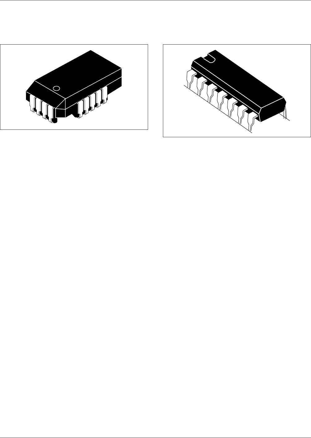
or ceramics (see Figure 13-1).
13.1 Termination Materials End terminations should be
solder coated with a tin/lead alloy or a lead free equivalent.
The solder should contain between 58 to 68% tin. Solder
may be applied to the termination by hot dipping or by
plating from solution. Plated solder terminations should be
subjected to a postplating reflow operation to fuse the sol-
der. The tin/lead finish should be at least 0.0075 mm
[0.0003 in] thick.
The termination shall be symmetrical, and shall not have
nodules lumps, protrusions, etc., that compromise the sym-
metry or dimensional tolerances of the part. The end termi-
nation shall cover the ends of the components, and shall
extend out to the top and bottom of the component.
Solder finish applied over precious metal electrodes shall
have a diffusion-barrier layer between the electrode metal-
lization and the solder finish. The barrier layer should be
nickel or an equivalent diffusion barrier, and should be at
least 0.00125 mm [0.00005 in] thick.
For lead free finishes a combination of tin, silver and cop-
per is the prevalent replacement for the tin/lead finish. Sol-
derability testing should be applied per IPC-J-STD-002 to
determine attachment capability of the applicable compo-
nent type.
13.2 Marking Parts shall be marked with the part num-
ber and a date code. In addition, pin 1 shall be identified.
13.3 Carrier Package Format Carrier format may be
tubes or as agreed to between user and vendor.
13.4 Resistance to Soldering The parts should be
capable of withstanding ten cycles through a standard
reflow system operating at 215 °C [419 °F]. Each cycle
shall consist of a minimum of 60 seconds exposure at
215T°C [419 °F]. See IPC/JEDEC J-STD-020 for appropri-
ate reflow cycles and profiles when using lead free solders.
IPC-7351-12-02
Figure 12-2 PLCCR Construction
IPC-7351-13-01
Figure 13-1 DIP Construction
IPC-7351 February 2005
56
标准分享网 www.bzfxw.com 免费下载
14 IPC-7358 AREA ARRAY COMPONENTS (BGA, FBGA,
CGA)
The area array device family includes square and rectangu-
lar package configurations and is furnished in a variety of
base materials. This device family includes Ball Grid Array
(BGA) parts (rigid, flexible or ceramic substrate); Fine
Pitch Ball Grid Array (FBGA) parts (rigid or flexible sub-
strate); and Column Grid Array (CGA) parts (ceramic sub-
strates).
The area array device families are generally marked with
the manufacturer’s name or symbol, part number, date code
and orientation mark in the corner near contact location A1.
Area array devices may be furnished in matrix tray or tape
and reel packaging formats. Tape and reel packaging is
generally preferred for high volume assembly. Plastic trays
and reels must be transported and stored in moisture proof
containers. When plastic array devices are exposed to the
environment for an extended period of time, moisture may
absorb into the device. The absorbed moisture, if excessive,
may expand (when exposed to higher temperatures typical
of reflow solder process), causing cracking and other
physical damage.
Area array devices are typically attached to the host inter-
face structure using eutectic solder alloy, however, optional
methods of attachment may include electrically conductive
epoxy or polymer. There is also a process difference
between the solder application for those terminations that
collapse slightly during soldering and those terminations
that do not collapse where a significant amount of addi-
tional solder paste is required. Array package assembly
should not require specialized equipment or processes
beyond that used for vision assisted SMT pick and place.
In conjunction with the proper land size, the volume of
solder paste application is a fundamental parameter to keep
under control in order to have a good reflow quality yield
and a reliable solder joint. Paste volume deposition may be
a matter of SPC adoption at print process step.
14.1 Area Array Configurations For additional detail on
package variations, mechanical feature dimensions and
allowable physical tolerances beyond the following sec-
tional descriptions, refer to the JEDEC Publication JEP95
and IPC-7095.
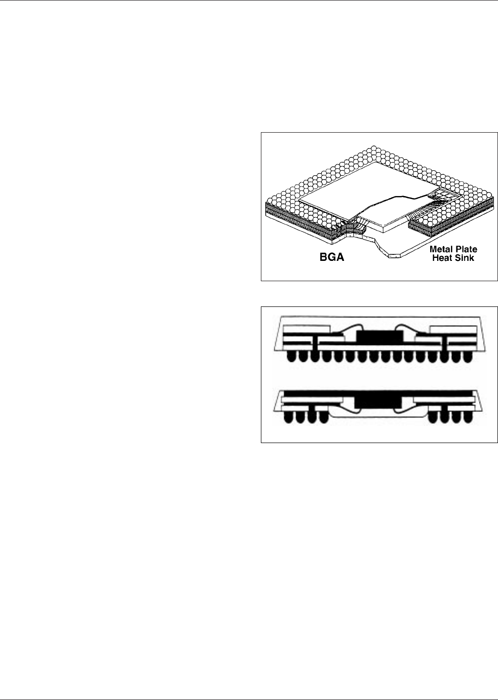
14.1.1 BGA Packages Figure 14-1 shows the elements
of a BGA. JEDEC Publication JEP95, Section 4.14, defines
a Ball Grid Array Package family. A Ball Grid Package
(BGA) is a square or rectangular 1.50 mm, 1.27 mm, &
1.00 mm pitch package with an array of metallic balls or
columns on the underside of the package. The main body
of the package has a metallized circuit pattern applied to a
dielectric structure. To this package body, the semiconduc-
tor die(s) is attached to either the top or bottom surface. On
the underside of the dielectric is an array pattern of metal-
lized balls/columns which form the mechanical and electri-
cal connection from the package body to a mating feature
such as a printed circuit board. The array contact material
will allow conventional reflow solder or other attachment
processes. The surface that contains the die may be encap-
sulated by various techniques to protect the semiconductor.
Figure 14-2 compares the top surface attached die to the
cavity down configuration.
14.1.1.1 Termination Materials The BGA ball termina-
tion may consist of a variety of metal alloys. Some of these
include balls with some lead content such as 37Pb63Sn,
90Pb10Sn, 95Pb5Sn, while others do not contain lead such
as Sn96.5Ag3.0Cu0.5, Sn96.5Ag3.5, Sn-9Zn-0.003Al. It is
a good recommendation to use the same alloy, in a paste
form, to attach the BGA balls to the mounting substrate;
however some of the balls that do not collapse require a
paste that is more conducive to reflow temperatures.
For lead free finishes a combination of tin, silver and cop-
per is the prevalent replacement for the tin/lead finish. Sol-
derability testing should be applied per IPC-J-STD-002 to
determine attachment capability of the applicable compo-
nent type.
14.1.1.2 Process Considerations BGAs are usually
processed using standard reflow solder processes. Parts
should be capable of withstanding three cycles through a
IPC-7351-14-01
Figure 14-1 Ball Grid Array (BGA) IC Package Example
IPC-7351-14-02
Figure 14-2 Example of Plastic BGA Package
Configurations
February 2005 IPC-7351
57
standard reflow system operating within a range of 235 °C
to 260 °C [455 °F to 500 °F] depending on the attachment
alloy being used. Each cycle shall consist of 60 to 90 sec-
onds exposure at the particular temperature selected. See
IPC/JEDEC J-STD-020 for appropriate reflow cycles and
profiles when using lead free solders.
It is important to consider that Plastic BGAs are moisture
sensitive device/components (MSD). Precaution must be
taken during the printed board assembly process in order to
avoid MSD damages (Delamination, Cracks, etc). Trace-
ability for baking PBGA, might be required mainly when
attached in a double sided/reflow printed board assembly.
14.1.2 Fine Pitch BGA Package (FBGA) JEDEC Publica-
tion JEP95, Section 4.5, defines a Fine-pitch Ball Grid
Array (FBGA) package is a reduced-pitch (<1.00 mm) ver-
sion of a Ball-Grid-Array (BGA) package. The carrier body
of the package has a metallized circuit pattern applied to a
dielectric structure. One or more semiconductor devices are
attached to either the top or the bottom surface of this
dielectric carrier. On the underside of the dielectric carrier
is an array pattern of metallized balls, which form the
mechanical and electrical connection from the package
body to a mating feature such as a printed circuit board.
The surface that contains the die may be encapsulated by
various techniques to protect the semiconductor. The
requirements for a square FBGA package family that
allows four optional contact pitch variations; 0.50, 0.65,
0.75 and 0.80 mm and defines four device profile (height)
variations as well. The 0.75 mm pitch has been added to
the list thus providing four pitch variations for FBGA type
parts.
The total profile height of the FBGA, as measured from the
seating plane to the top of the component, is greater than
1.70 mm. The Low-Profile Fine-Pitch Ball-Grid-Array
(LFBGA) and is a reduced-height version of an FBGA.
The total profile height of the LFBGA as measured from
the seating plane to the top of the component, is no greater
than 1.20 mm. Thin-Profile Fine-Pitch Ball-Grid-Array
(TFBGA) is a reduced-height version of an FBGA with a
total profile height as measured from the seating plane to
the top of the component that does not exceed 1.00 mm
and the Very-Thin-Profile Fine-Pitch Ball-Grid-Array
(VFBGA) is a reduced-height version of an FBGA with a
total profile height as measured from the seating plane to
the top of the component that is at or below 0.80 mm.
The JEDEC design guide for FBGA allows the manufac-
turer the option to increase ball diameter as the spacing or
pitch between ball contact centers increase as compared in
Table 14-1. As of this release JEDEC standards do not
support the 0.75 mm pitch, however the industry has some
parts available in that pitch.
The larger ball diameter option has been allowed to accom-
modate packages using rigid interposer structures. The
larger diameter ball may compensate to a degree, for the
wide mismatch of the coefficient of thermal expansion
(CTE) between the silicon die and the rigid PCB structure.
Fine pitch ball parts may require special processing outside
the normal pick/place and reflow manufacturing operations.
This requirement relates to the amount of solder paste, the
precision of the placement machine and the soldering pro-
cess profile, to permit all parts to become attached at the
same time that the FBGA is reflowed.
Ball termination and process considerations for FBGA are
the same as that for BGA as described in 14.1.1.1 and
14.1.1.2.
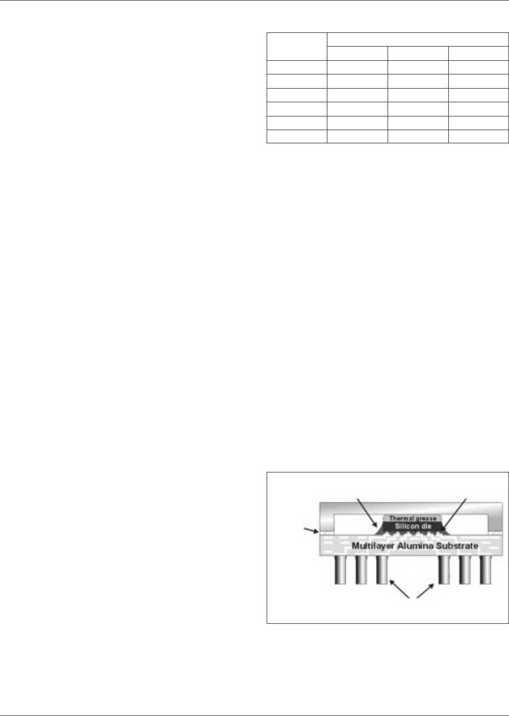
14.1.3 Ceramic Column Grid Arrays (CGA) Solder col-
umn contacts typical of that illustrated in Figure 14-3 are
used for larger ceramic-based packages (32.0 mm to 45.0
mm). The package resembles the earlier pin-grid-array but
with closer contact pitch and more fragile leads (columns).
The column contact diameter is approximately 0.5 mm
with its length varying from 1.25 mm to 2.0 mm. The col-
umns are attached to the package either by eutectic
(Sn63Pb37) solder or they are cast in place using 90% Pb
and 10% Sn.
The longer columns typically increase solder joint reliabil-
ity by absorbing a great deal of the stresses created by the
CTE mismatch between the ceramic package and the
board. Longer columns, on the other-hand, may reduce
Table 14-1 JEDEC Standard JEP95
Allowable Ball Diameter Variations for FBGA (mm)
Ball Pitch
Ball Diameter
Minimum Nominal Maximum
0.80 0.45 0.50 0.55
0.80 0.35 0.40 0.45
0.80 0.25 0.30 0.35
0.65 0.35 0.40 0.45
0.65 0.25 0.30 0.35
0.50 0.25 0.30 0.35
IPC-7351-14-03
Figure 14-3 Ceramic Column Grid Array (CGA) Package
(Cross-Sectional View)
Solder Columns
(Sn10Pb90)
Underfil
Solder Balls
(Sn5Pb95)
Sealing
Adhesive
IPC-7351 February 2005
58
标准分享网 www.bzfxw.com 免费下载