IPC-7351-2005_表面贴装焊盘布局设计和标准通用要求.pdf - 第39页
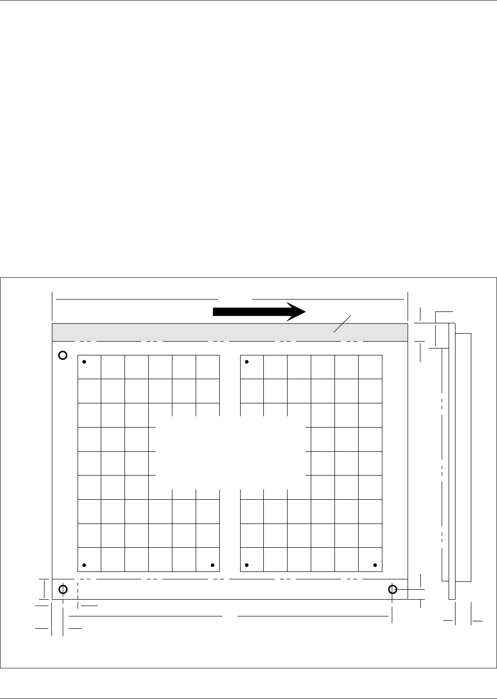
www.bzfxw.com the board handling and fixturing equipment. These dimen- sions should be obtained from the process equipment manufacturer before board or panel design (see Figure 3-19). Special tooling and fixturing holes ar…
www.bzfxw.com
IPC-7351-3-17
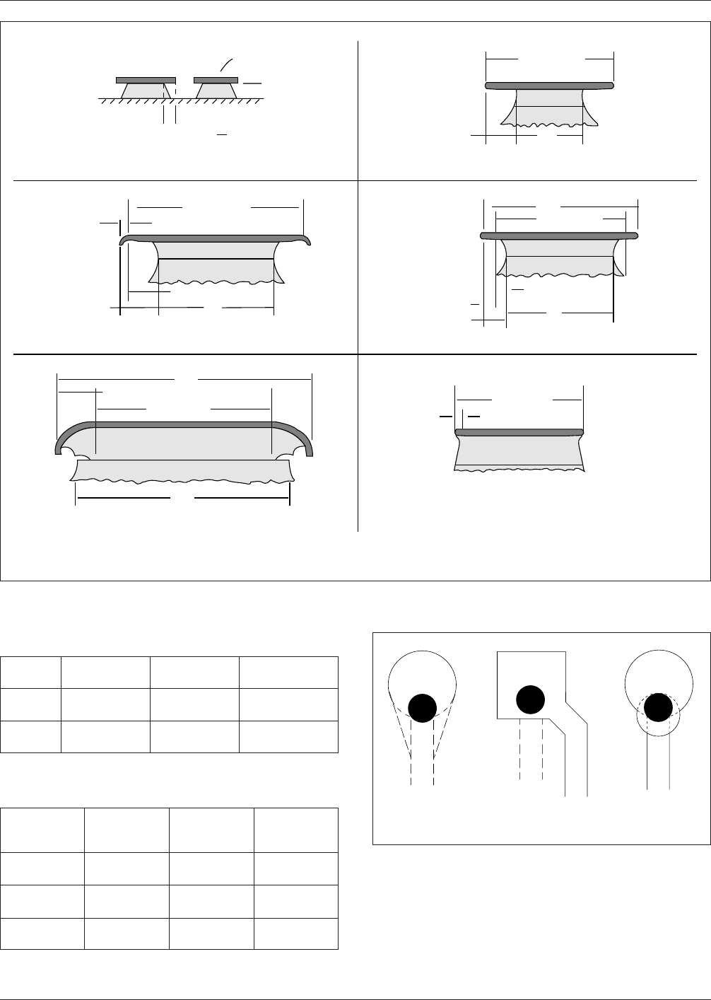
Figure 3-17 Conductor Description
▼
LaminateX
▼
Etch Factor =
V
X
An etch factor of 1/1 is usually considered practical.
Higher factors may be specified for some applications.
Resist
▼
V
▼
▼
"B" (DCW)
"E" Outgrowth
▼
▼
▼
▼
▼
▼
▼
"C" Undercut
▼
"A"
(MCW)*
Overhang
Panel Plating (Liquid Resist)
▼
▼
(OCW)*
▼
▼
"D"
"B" (DCW)*
"E" Outgrowth
▼
▼
(MCW)*
"A"
▼
▼
Pattern Plating (Liquid Resist)
▼
"B" (DCW)
(MCW)*
"C" Undercut
& Overhang
Panel Plating (Dry Film Resist)
▼
▼
"A"
▼
▼
▼
▼
▼
"D"
▼
"A"
(MCW)*
Overhang
Pattern Plating (Dry Film Resist)
▼
▼
▼
(OCW)*
"B" (DCW)*
▼
▼
▼
▼
"E" Outgrowth
▼
▼
"C" Undercut
▼
▼
"B" (DCW)*
▼
"C" Undercut
▼
Thin Clad & Pattern Plating (Dry Film Resist)
A = MCW (Minimum Conductor Width) B = DCW (Design Conductor Width) D = OCW (Overall Conductor Width)
Table 3-17 Conductor Width Tolerances,
0.046 mm [0.00181 in] Copper, mm [in]
Feature
Producibility
Level A
Producibility
Level B
Producibility
Level C
Without
plating
± 0.06 mm
[± 0.00236 in]
± 0.04 mm
[± 0.00157 in]
± 0.015 mm
[± 0.0005906 in]
With
plating
± 0.10 mm
[± 0.00393 in]
± 0.08 mm
[± 0.00314 in]
± 0.05 mm
[± 0.0197 in]
Table 3-18 Feature Location Accuracy (units: mm [in])
Greatest
Board/ X,Y
Dimension
Producibility
Level A
Producibility
Level B
Producibility
Level C
Up to 300
[11.81]
0.30
[0.012]
0.20
[0.00787]
0.10
[0.00394]
Up to 450
[17.72]
0.35
[0.0138]
0.25
[0.00984]
0.15
[0.00591]
Up to 600
[23.62]
0.40
[0.0157]
0.30
[0.012]
0.20
[0.00787]
IPC-7351-3-18
Figure 3-18 Examples of Modified Landscapes
Corner Entry
Filleting
Key Holing
IPC-7351 February 2005
28
标准分享网 www.bzfxw.com 免费下载
www.bzfxw.com
the board handling and fixturing equipment. These dimen-
sions should be obtained from the process equipment
manufacturer before board or panel design (see Figure
3-19).
Special tooling and fixturing holes are generally located
within the edge clearance areas. The clearance areas are
needed to avoid interference with board handling fixtures,
guidance rails and alignment tools.
For accurate fixturing, two or more nonplated holes are
located in the corners of the board to provide accurate
mechanical registration on board transfer equipment. Board
handling holes (typically 3.2 mm [0.126 in]) may also be
located in the clearance areas. These holes may be used by
automated board handling equipment or for test fixture
alignment. Specific panel size should be obtained from the
equipment manufacturer or process engineer.
3.4.8.1 Board Size and Panel Construction In order to
fully utilize the automation technology associated with
surface mount components, a designer should consider how
a printed board or P&I structure will be fabricated,
assembled and tested. Each of these processes, because of
the particular equipment used, may require fixturing, which
will affect or dictate certain facets of the board layout.
Tooling holes, panel size, component orientation and clear-
ance areas (both component and conductor) on the primary
and secondary sides of the board are all equipment and
process dependent.
To produce a cost-effective layout through optimum base
material utilization, a designer should consult with the
board manufacturer to determine optimum panel size. The
board should be designed to utilize the manufacturer’s sug-
gested usable area. Smaller boards can be ganged or nested
in a uniform panel format to simplify fixturing and reduce
excessive handling during assembly. Panel layout is typi-
cally defined by an assembly process specialist or the
manufacturing service provider.
IPC-7351-3-19
Figure 3-19 Typical Copper Glass Laminate Panel
▼
The keepout zone defined in this illustration is typical for in-line assembly automation using reflow and wave solder processes.
▼
X
Typical Finished Panel
for Automated SMT
Assembly Equipment
Showing two
Printed Board Assemblies
▼
300mm
[12.0 in]
▼
▼
3.0mm
[0.12 in]
▼
▼
5.0 mm
[2.0 in]
▼
10 mm [0.40 in]
▼
5 mm [0.20 in]
▼▼
▼
3.0 mm
[0.12 in]
Keep Clear
▼
Primary Component Side
Secondary Component Side
▼
▼
12.0 mm
max.
[0.500 in]
5mm
[2.0 in] min.
DIRECTION OF FLOW
KEEPOUT ZONE
KEEPOUT ZONE
▼
▼
▼
February 2005 IPC-7351
29
www.bzfxw.com
Panel construction may include several boards arranged in
a matrix or simply one board requiring additional material
retained for efficient assembly processing. The large board
or several smaller boards are retained in the panels and
separated after all assembly processes are completed.
Excising or separating the individual boards from the panel
must be planned as well. Several methods are used to retain
circuits in a panel, including V-groove scoring, NC routing
and routed slot with break-away tabs.
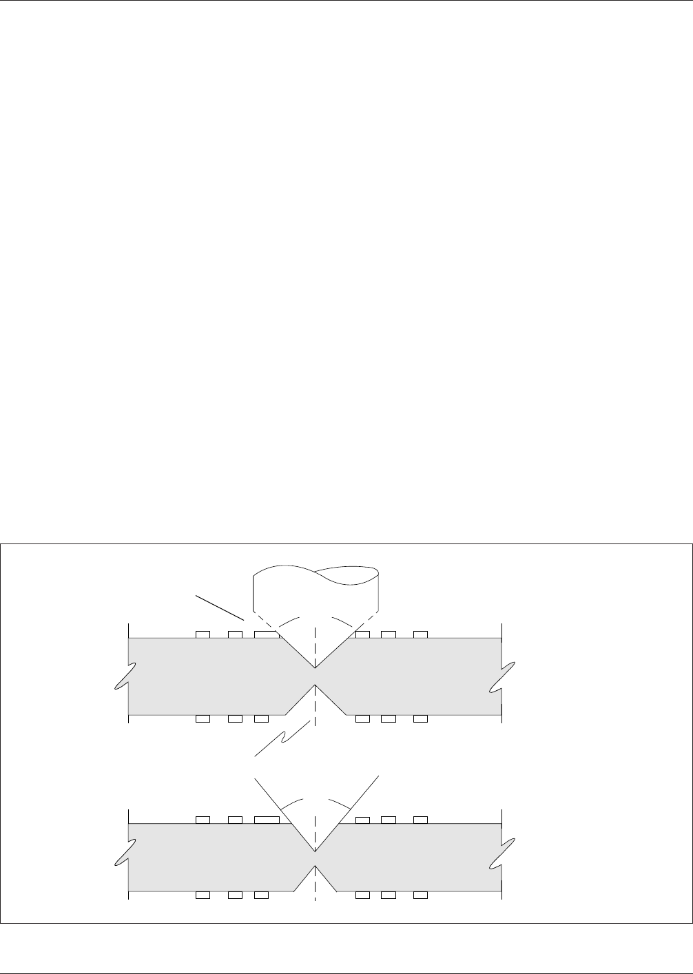
3.4.8.2 V-Groove Scoring V-groove scoring may be pro-
vided to enable post assembly separation. The groove fea-
ture is generally provided on both surfaces of the board and
only in a straight line. A small cross-section of board mate-
rial is retained at the break line. An allowance for the scor-
ing angle must be made as well. Conductors that are
located too close to the score groove will be exposed or
damaged, and rough edges must be sanded lightly to
remove burrs and rough fabric particles (see Figure 3-20).
3.4.8.3 Routed Slot and Tab Features The routed slot
and tab pattern is widely used for panel construction and
break-away tab extensions. Routing is more precise than
scoring, and edge surfaces are smooth, but the break-away
‘‘tab’’ points will require consideration. Tabs can be cut
and ground flush with the board edge or predrilled in a pat-
tern. The drilled pattern furnishes a low stress break point
on the ‘‘tab.’’ If the hole pattern is recessed within the
board edge, secondary sanding or grinding can be bypassed
(see Figure 3-21).
3.5 Outer Layer Surface Finishes
3.5.1 Solder Mask Finishes
Solder mask coatings are
used to protect the circuitry on the printed board. Solder
mask coatings are available in two forms, liquid and dry
film. The polymer mask material is applied using several
process methods and is furnished in varying thicknesses.
As an example, liquid materials will have a finished thick-
ness of 0.02 mm [0.0079 in] to 0.025 mm [0.00984 in]
while the dry film products are supplied in thicknesses of
0.04 mm [0.016 in], 0.08 mm [0.0315 in], and 0.10 mm
[0.0394 in]. Although screen type printing for solder mask
is available, photo-imaged soldermask is recommended for
surface mount applications.
The photo process provides a precise pattern image and
when properly developed eliminates mask residue from
land pattern surfaces. The mask thickness may not be a
factor on most surface mount assemblies but, when fine
pitch (0.63 mm [0.0248 in] or less) IC devices are mounted
on the printed boards, the lower profile soldermask will
provide better solder printing control.
3.5.2 Solder Mask Clearances A solder mask may be
used to isolate the land pattern from other conductive fea-
tures on the board such as vias, lands or conductors. Where
no conductors run between lands, a simple gang mask
opening can be used as shown in Figure 3-22.
For land pattern designs with routed conductors between
lands (see Figure 3-23), the solder mask pattern must
IPC-7351-3-20
Figure 3-20 Conductor Clearance for V-Groove Scoring
90˚
▼
▼
Break Line
▼
60˚
▼
▼
Conductors Must
Be Clear of Score
Zone
90˚ Score
Option
60˚ Score
Option
▲
IPC-7351 February 2005
30
标准分享网 www.bzfxw.com 免费下载