IPC-7351-2005_表面贴装焊盘布局设计和标准通用要求.pdf - 第43页
Determining the percentage of nodal access to design into a board layout requires trading of f all the issues discussed previously: defect rate, test development cost, test opera- tion costs including manual troubleshoot…
5 TESTABILITY
5.1 Board and Assembly Test
There are five basic types
of tests which can be performed on SMT boards. These
are:
a) Bare-board test which checks the unpopulated board for
shorts and opens
b) Manufacturing defect analysis which checks the popu-
lated board for soldering shorts
c) In-circuit test operational verification of each individual
component
d) Functional test operational verification of functional
block of circuits
e) Combinational test limited integration of in-circuit and
functional test
The first test type is a bare-board test performed by the
board fabricator. The remaining four test types are loaded
on assembled board tests and performed after assembly.
The bare-board test should be mandatory, while the loaded
board may be tested using any one or a combination of the
four loaded board tests.
5.1.1 Bare-Board Test In testing printed boards using
through-hole technology, the defect rate and the test meth-
ods chosen are the principle determiners of overall test
cost. Real-estate considerations (specifically the percentage
of nodes that are available for bed-of-nails probing) are not
a concern, since the holes provide 100% nodal access. In
testing surface mount boards, however, real-estate consid-
erations (in addition to defect rates) have an impact on test
costs, since nodal access determines which test methods
are possible and effective.
The use of design concepts with grid-based 100% nodal
access from either side of the board may be the most eco-
nomical approach from the total process perspective. If the
grid-based test land concept is used, the test fixtures for
bare and assembled board tests will not become obsolete
through later board connectivity revisions if the test nodes
are not moved. Also, if the printed board uses buried vias,
the grid-based test land concept with 100% nodal access
may provide access to buried nets from the ends of the
nets; this is a benefit realized during the bare-board test.
5.1.2 Assembled Board Test The method of test must
be determined prior to design layout. If the defect rate is
relatively high, most boards will require diagnosis, and the
economics of automatic in-circuit test (ICT) will demand
that full nodal access be provided within the board layout.
If the defect rate is low, ICT may be omitted and rely on a
functional test. Extremely low defect levels would theoreti-
cally allow 0 % nodal access (no bed-of-nails test at all),
applying only a simple pass/no-pass test through a common
interface connector.
The major considerations in determining nodal access are:
• Defect rate.
• Diagnostic capability.
• Real-estate impact.
• Board area.
• Layer count.
• Cost impact.
IPC-7351-4-01
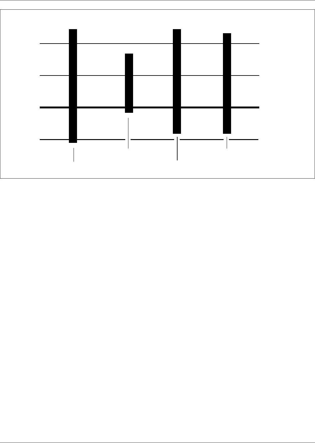
Figure 4-1 Component Operating Temperature Limits
125
85
125
120
0˚C
–40–40
–10
–55
Ceramic ICs
Plastic ICs
Capacitors
Resistors
▼ ▼
▼
▼
IPC-7351 February 2005
32
标准分享网 www.bzfxw.com 免费下载

Determining the percentage of nodal access to design into
a board layout requires trading off all the issues discussed
previously: defect rate, test development cost, test opera-
tion costs including manual troubleshooting costs, and, of
course, impacts on real estate. Short of having no defects
at all, full nodal access remains the most desirable option.
As with through-hole technology boards, once the board is
designed (nodal access fixed) and its tests are designed
(test methods fixed), the defect rate becomes the primary
key to reducing test costs. Therefore, defect reporting,
analysis, and correction/prevention are imperative. This
may involve closer supplier relationships to reduce compo-
nent and board level problems, and in-house action to
reduce process-induced problems.
5.2 Nodal Access In the early stages of product develop-
ment cycles, test philosophies and strategies are often
undefined. This is especially true when a company is mov-
ing from one level of packaging technology to the next
higher level of packaging technology, for example, from
through-hole technology to surface mount technology or
from fine-pitch lead-frame packaged ICs to BGA or CSP.
During these transition periods, the concurrent engineering
approach is essential for designing nodal access for test-
ability into the product. Concurrent engineering is the prin-
ciple vehicle by which test priorities can and should be
moved up to the beginning of the design cycle and
addressed with a higher priority. In the early stages of a
design, a test philosophy should be clearly defined, then a
strategy for executing the tests can be implemented. An
ideal philosophy to adopt is one that identifies all of the
different test types and the level of test that each type
requires.
5.2.1 Test Philosophy The test philosophy should be
written to encompass whatever combination of tests are
necessary for the product. Then, a simple strategy for
implementing the required tests can be defined prior to
beginning the design process. Planning testability at the
beginning of a product development cycle instead of the
end can result in significantly lower test costs per node and
provide higher nodal accessibility throughout the entire
process from initial design to final test.
The best test philosophy to adopt is one that will make
provisions for executing every test method available. Even
when the product testing procedure is well defined at the
beginning of the development cycle, it may change after
the design is complete. Some things to consider in outlin-
ing a test philosophy:
a) Strategic placement of all component vias.
b) Provide access to every node of every net.
c) Access of every node from one side of the board is pre-
ferred.
d) Correct test pad geometries and clearances.
Even in the higher density designs, the philosophy of pro-
viding 100% access to every node of every net from either
side of the board can be accomplished. However, this deci-
sion must be made at the beginning of a design.
5.2.2 Test Strategy for Bare Boards After the product
test philosophy has been established, a test strategy or pro-
cedure can be defined. For an overview of several elements
of a procedure, consider the following:
a) Vision inspection of inner layers using AOI.
b) Vision inspection of O/L land/via connections.
c) Probe only vias on either side for bare board test.
d) Do not damage SMT lands with probe tips.
e) Probe secondary side vias for loaded test board.
f) Screen paste on vias for airtight board.
The actual product test strategy must be organized by all of
the concurrent engineering team members who will be
involved in the testing process. This will ensure that the
integration of the various test types and procedures will not
have too much redundancy, or create gaps that may endan-
ger test integrity.
5.3 Full Nodal Access for Assembled Board The num-
ber of test probes needed to test the board is equal to the
total number of device nodes or common connection
between devices. However, in the case of most dense sur-
face mount designs, this often requires the use of a double-
sided, or clamshell test fixture because all of the nodes are
not accessible from one side of the board.
In-Circuit Test (ICT) only needs to have access to one node
per net. Every net has at least two nodes. Some nets have
many nodes, for example, on memory boards one net may
be connected to many nodes. In order to achieve full integ-
rity at the ICT level, access to only one node of each net is
all that is required. Therefore, the total number of test
probes required to perform the ICT is significantly less
than the number required for the bare board test.
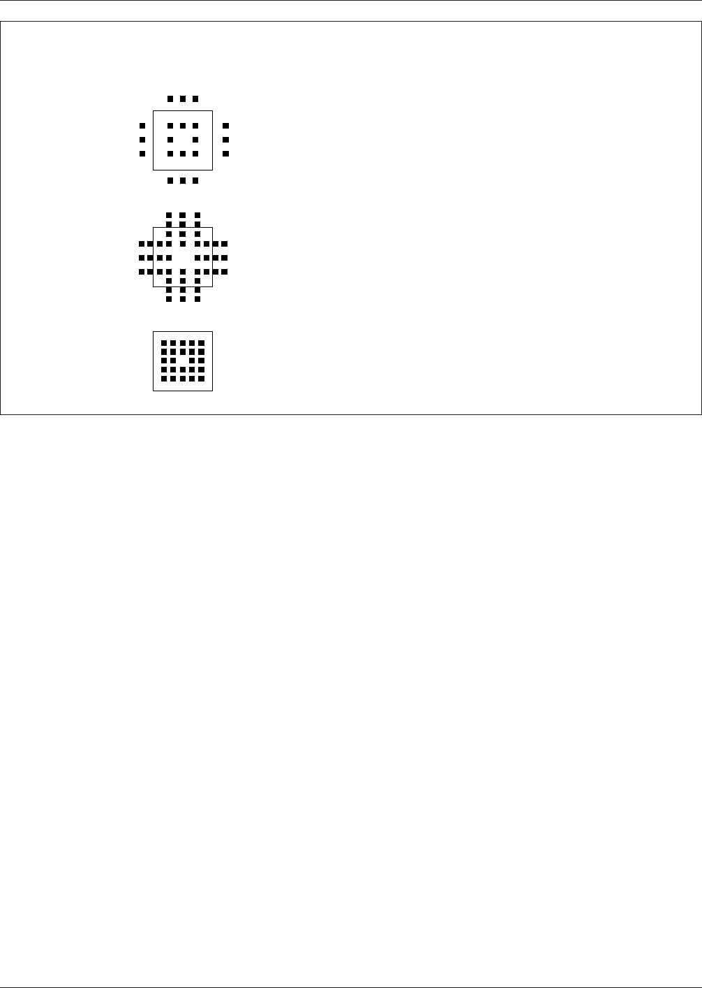
For fine-pitch components, it is good design practice to
distribute approximately half of the test vias to the inside
of the land pattern and the other half to the outside of the
land pattern as shown in Figure 5-1. This accomplishes two
objectives:
1. The maximum density of test points established for a
given piece of test equipment is not exceeded.
2. Wider distribution of test points reduces the high-
pressure point areas which cause fixture bowing during
vacuum or mechanical actuation.
5.3.1 In-Circuit Test Accommodation Specific via lands
and holes can be reserved and accessed for automatic
in-circuit test (ICT). The via land location for each com-
mon network in a circuit is matched to a test probe contact
February 2005 IPC-7351
33
in the test fixture. The test system can then drive each
device on the assembly and quickly locate defective
devices or identify assembly process problems.
To insure precise alignment of the probe contact pins with
the printed board, exact x and y probe position and specific
networks must be furnished to the fixture developer. Iden-
tifying the test locations as components in the CAD data-
base will allow for easy transfer of fixture drilling data.
This data will reduce fixture development time and elimi-
nate the drilling of excessive, nonfunctional holes in the
fixture base. For low volume assembly, or high component
density assembly, fixtureless testing by way of flying probe
equipment is an option.
5.3.2 Multi-Probe Testing Some test probe systems can
exert considerable deformation forces on the assembled
boards and are a known source of premature service fail-
ures. An essential part of the printed board layout is to
ensure that the location of probing points on the board are
staggered at sufficient distances to avoid excessive defor-
mation during multi-probe testing. When the probe point
locations are highly concentrated, additional support may
be needed in the test fixture design in order to counter the
effect against the high probe pressure concentration. The
area on the board where the support is to be provided
should be located where it is clear of conductors and com-
ponents.
5.4 Limited Nodal Access Provided the designer has
allowed sufficient room for access to the test land(s), lim-
ited nodal access (less than 100%) still allows the use of
spring probe (bed-of-nails) testing, but not as effectively as
full nodal access does. When nodal access is less than
100%, shorts, defects and in-circuit testing cannot be per-
formed completely, and some faults may not be detected.
A greater burden is therefore placed on functional or sys-
tem test to detect and diagnose shorts, defects, and bad
devices. This burden varies inversely with the nodal access
percentage. The extra effort at functional test may consist
of additional recurring manpower cost to diagnose failing
boards, or it may mean developing a more detailed func-
tional test (nonrecurring cost) than would have been
planned otherwise.
5.5 No Nodal Access No nodal access (0%) prohibits
bed-of-nails testing and defers all assembly defects and
component testing until the functional or system test bed.
This can only be cost-justified if the much higher cost-per-
defect repair is performed so infrequently that the total cost
is less than the cost of developing and operating an ATE
bed-of-nails test. In other words, the first pass yields must
be extremely high to justify this approach.
5.6 Clam-Shell Fixtures Impact Probing the printed
board from both sides requires a ‘‘clam-shell’’ type of fix-
ture. These are expensive, take more time to fabricate,
require larger test lands on the primary side to protect
against registration problems due to tolerance stack-ups,
and they are more difficult to maintain.
IPC-7351-5-01
Figure 5-1 Test Via Grid Concepts
Test Via Grid Concepts
1.25 mm Pitch Component
2.5 mm Via Test Grid
1.25 mm Pitch Component
1.25 mm Via Test Grid
0.63 mm Pitch Component
1.25 mm Via Test Grid
Preferred
Acceptable
Poor Design
IPC-7351 February 2005
34
标准分享网 www.bzfxw.com 免费下载