IPC-7351-2005_表面贴装焊盘布局设计和标准通用要求.pdf - 第76页
P acka ge Outline Component Examples Zero Rotation Pin 1 on Left Side Land P attern Note: Pin 1 is always the ''P ositive Pin'' Chip Components Chip Capacitor Chip Resistor Chip Inductor Molded Capaci…

15.3.2 Carrier Package Format The carrier package for-
mat for the SON includes anti-static tubes, since the units
have no leads that can bend, as well as conductive carrier
tape and reel.
15.3.3 Process Considerations The SON package is
resistant to failure from board bending (flexing); it features
a metal bottom paddle, which can be soldered directly to
the PC board. This adds adhesive strength while avoiding
messy epoxy under-fill. Though not required, it is highly
recommended that this bottom paddle be soldered to the
printed board, especially for printed boards with significant
flex. For the more flex-resistent printed boards, the bottom
paddle soldering is not necessary but is recommended due
to CTE stresses and possible ground signals through the
bottom paddle.
15.3.4 Solder Resist Considerations The solder resist
opening should be 120 µm to 150 µm larger than the land
size resulting in 60 µm to 75 µm clearance between the
copper land and solder resist. This allows for solder resist
registration tolerances, which are typically between 50 µm
to 65 µm, depending upon the board fabricators’ capabili-
ties. Typically each land on the PCB should have its own
solder resist opening with a web of solder resist between
two adjacent lands. Since the web has to be at least 75 µm
in width for solder resist to adhere to the PCB surface, each
land can have its own solder resist opening for lead pitch
of 0.5 mm or higher, based on the land width dimensions.
However, for 0.4 mm pitch parts with PCB land width of
0.25 mm, not enough space is available for solder resist
web in between the land. In such cases, it is recommended
to use the ‘‘gang’’ type solder resist opening shown in
Figure 3-22 where a big opening is designed around all
land on each side of the package with no solder resist in
between the land.
16 ZERO COMPONENT ORIENTATIONS
The zero component orientations expressed in IPC-7351
are defined in terms of the standard component CAD
library with respect to a given PCB design. Recognizing
that a single land pattern may be used for the same compo-
nent part from different suppliers and that each component
supplier may have different orientations on their reels or
that the components may come in trays, there exists the
possibility that the PCB designer loses the ability to refer-
ence a single land pattern if the zero rotation of a part is
according to the method the component is delivered to the
assembly machine. Since the CAD library contains a single
land pattern, the zero component rotation is thus defined
according to the CAD library. Subsequently, component
suppliers can identify the orientation of the parts on the
reels by associating the placement of the part on the reel to
zero orientations defined in IPC-7351. If pin 1 is at the
lower left as defined by the pick and place machine tape
and reel, for example, then the component on the reel is
rotated 90° counterclockwise from the zero rotation given
in IPC-7351. Standardizing the orientation of components
for the installation and utilization of various packaging
methods, such as tubes, trays or tapes and reels, among the
variations of automated assembly equipment existing today
is outside the scope of this document.
Figure 16-1 lists the most commonly used parts and their
proper zero component rotation.
February 2005 IPC-7351
65
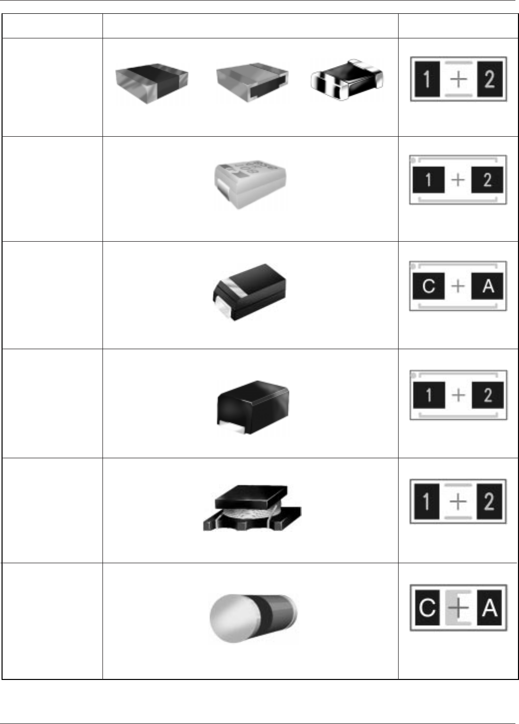
Package Outline Component Examples
Zero Rotation
Pin 1 on Left Side
Land Pattern
Note: Pin 1 is always
the ''Positive Pin''
Chip
Components
Chip Capacitor
Chip Resistor Chip Inductor
Molded
Capacitors
Pin 1 on Left Side
Land Pattern
Note: Pin 1 is always
the ''Positive Pin''
Pin 1 on Left Side
Land Pattern
Note: Pin 1 is always
the ''Positive Pin''
Precision Wire
Wound
Components
Pin 1 on Left Side
Land Pattern
Note: Pin 1 is
always the
Cathode
MELF
Diodes
Molded
Inductors
Pin 1 on Left Side
Land Pattern
Note: Pin 1 is always
the ''Positive Pin''
Molded
Diodes
Pin 1 on Left Side
Land Pattern
Note: Pin 1 is always
the Cathode
Figure 16-1 Zero Component Rotations for Common Package Outlines
IPC-7351 February 2005
66
标准分享网 www.bzfxw.com 免费下载
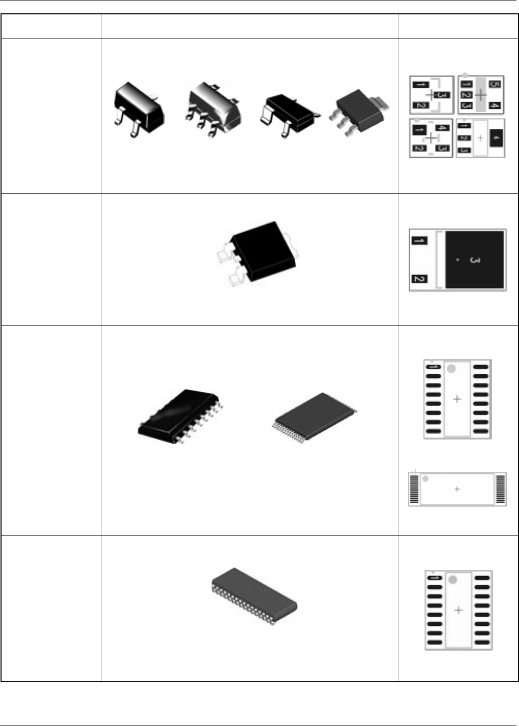
Pin 1 on Upper Left
Small Outline
Gullwing
Components
Small Outline
J-Lead
Components
Land Pattern
Pin 1 on Upper Left
SOIC, SOP & SOIC
TSSOP
Pin 1 on Upper Left
Land Pattern
Package Outline Component Examples
Zero Rotation
Land Pattern
SOIC J-Lead
Pin 1 on Upper Left
Land Pattern
SOT
Components
Pin 1 on Upper Left
Land Pattern
TO
Components
SOT23-3
SOT23-5
SOT343 SOT223
TO252 (DPAK)
Figure 16-1 Zero Component Rotations for Common Package Outlines (continued)
February 2005 IPC-7351
67