IPC-7351-2005_表面贴装焊盘布局设计和标准通用要求.pdf - 第56页
8.4.1 Basic Construction See Figure 8-5. 8.4.2 Marking Parts are available with or without marked capacitance values. 8.4.3 Carrier Package Format Bulk rods, 8 mm tape/4 mm pitch is preferred for best handling. T ape and…
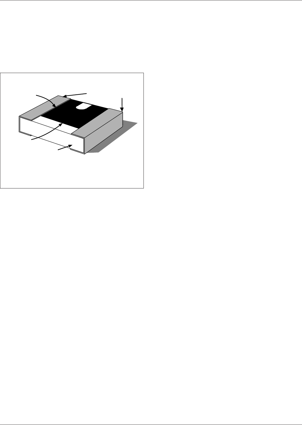
8.1.1 Basic Construction The resistive material is
applied to a ceramic substrate and terminated symmetri-
cally at both ends with a ‘‘wrap around’’ metal U-shaped
band. The resistive material is face-up, thus trimming to
close tolerances is possible. Since most equipment uses a
vacuum-type pickup head, it is important that the surface of
the resistor is made flat after trimming, otherwise vacuum
pickup might be difficult (see Figure 8-2).
8.1.2 Marking Resistors equal to or larger than 2012
[0805] are labeled. Resistors smaller than 1608 [0603] are
generally unlabeled.
8.1.3 Carrier Package Format Bulk rods, 8 mm tape/4
mm pitch is preferred for best handling. Tape and reel
specifications provide additional requirements.
8.1.4 Resistance to Soldering Parts should be capable
of withstanding five cycles through a standard reflow sys-
tem operating at 215 °C [419 °F]. Each cycle shall consist
of 60 seconds exposure at 215 °C [419 °F]. Parts must also
be capable of withstanding a minimum of 10 seconds
immersion in molten solder at 260 °C [500 °F]. See IPC/
JEDEC J-STD-020 for appropriate reflow cycles and pro-
files when using lead free solders.
8.2 Chip Capacitors (CAPC) A variety of values exist for
capacitors. This section describes the most common types.
8.2.1 Basic Construction Multilayer ceramic capacitors
use substrate materials such as alumina for hybrid circuits
and porcelainized metal. The monolithic construction used
in producing these chips results in a solid block of ceramic
with an enclosed electrode system and metallized ends for
circuit attachment. This solid block is rugged and capable
of withstanding the harsh environment and treatment asso-
ciated with manufacturing processes (see Figure 8-3). Elec-
trodes are given a common terminal by coating the chip
ends with a precious metal-glass formulation suspended in
an organic vehicle. Consecutive drying and firing elimi-
nates the organic components and affects a bond between
the ceramic dielectric and glass constituent in the termina-
tion.
8.2.2 Marking Ceramic capacitors are typically
unmarked.
8.2.3 Carrier Package Format Bulk rods, 8 mm tape/4
mm pitch is preferred for best handling. Tape and reel
specifications provide additional requirements.
8.2.4 Resistance to Soldering Parts should be capable
of withstanding five cycles through a standard reflow sys-
tem operating at 215 °C [419 °F]. Each cycle shall consist
of 60 seconds exposure at 215 °C [419 °F]. Parts must also
be capable of withstanding a minimum of 10 seconds
immersion in molten solder at 260 °C [500 °F].
Caution should be exercised when using the 4564 [1825]
capacitor mounted on organic substrates due to CTE mis-
match if the assembly sees wide temperature swings in the
assembly process or end use. See IPC/JEDEC J-STD-020
for appropriate reflow cycles and profiles when using lead
free solders.
8.3 Inductors (INDC, INDM, INDP) A variety of values
exist for inductors. This section describes the most com-
mon types.
8.3.1 Basic Construction At the time of publication,
there was no industry standard document for leadless
inductors. The dimensions were taken from manufacturer’s
catalogs, but only when at least two component vendors
manufacture the same package. However, the same induc-
tor value may not be available in the same package from
the two manufacturers (see Figure 8-4).
8.3.2 Marking Parts are available with or without
marked inductance values.
8.3.3 Carrier Package Format Bulk rods, 8 mm tape/4
mm pitch is preferred for best handling. Tape and reel
specifications provide additional requirements.
8.3.4 Resistance to Soldering Parts should be capable
of withstanding five cycles through a standard reflow sys-
tem operating at 215 °C [419 °F]. Each cycle shall consist
of 60 seconds exposure at 215 °C [419 °F]. Parts must also
be capable of withstanding a minimum of 10 seconds
immersion in molten solder at 260 °C [500 °F]. See IPC/
JEDEC J-STD-020 for appropriate reflow cycles and pro-
files when using lead free solders.
8.4 Tantalum Capacitors (CAPT) A variety of values
exist for tantalum capacitors. This section describes the
most common types.
IPC-7351-8-02
Figure 8-2 Chip Resistor Construction
Resistor
Alumina Chip
Platinum-Silver
Wrap-Around
Termination
Wire Bond Construction
Glass
Passivation
February 2005 IPC-7351
45
8.4.1 Basic Construction See Figure 8-5.
8.4.2 Marking Parts are available with or without
marked capacitance values.
8.4.3 Carrier Package Format Bulk rods, 8 mm tape/4
mm pitch is preferred for best handling. Tape and reel
specifications provide additional requirements.
8.4.4 Resistance to Soldering Parts should be capable
of withstanding five cycles through a standard reflow sys-
tem operating at 215 °C [419 °F]. Each cycle shall consist
of 60 seconds exposure at 215 °C [419 °F]. Parts must also
be capable of withstanding a minimum of 10 seconds
immersion in molten solder at 260 °C [500 °F]. See IPC/
JEDEC J-STD-020 for appropriate reflow cycles and pro-
files when using lead free solders.
IPC-7351-8-03
Figure 8-3 Chip Capacitor Construction
1. Termination
2. Dielectric
3. Electrode
4. Chip Length
5."A" Electrode Print
6. Electrode Print
7. Cap (Topping Layer)
8. End Margin
9. Base Layer
10. Shim (Active Dielectric Layer)
11. Side Margin
12. Chip Thickness
13. Chip Width
14. Termination Width
1
2 3
5
6
7
8
9
10
11
4
14
13
12
IPC-7351-8-04
Figure 8-4 Inductor Construction
Ferrite
Chip
▼
Precision Wire—Wound Molded
External
Electrode
▼
IPC-7351-8-05
Figure 8-5 Tantalum Capacitor Construction
or
IPC-7351 February 2005
46
标准分享网 www.bzfxw.com 免费下载
8.5 Metal Electrode Face Diodes (DIOMELF, RES-
MELF)
Resistors, ceramic capacitors, and tantalum
capacitors may all be packaged in these tubular shapes.
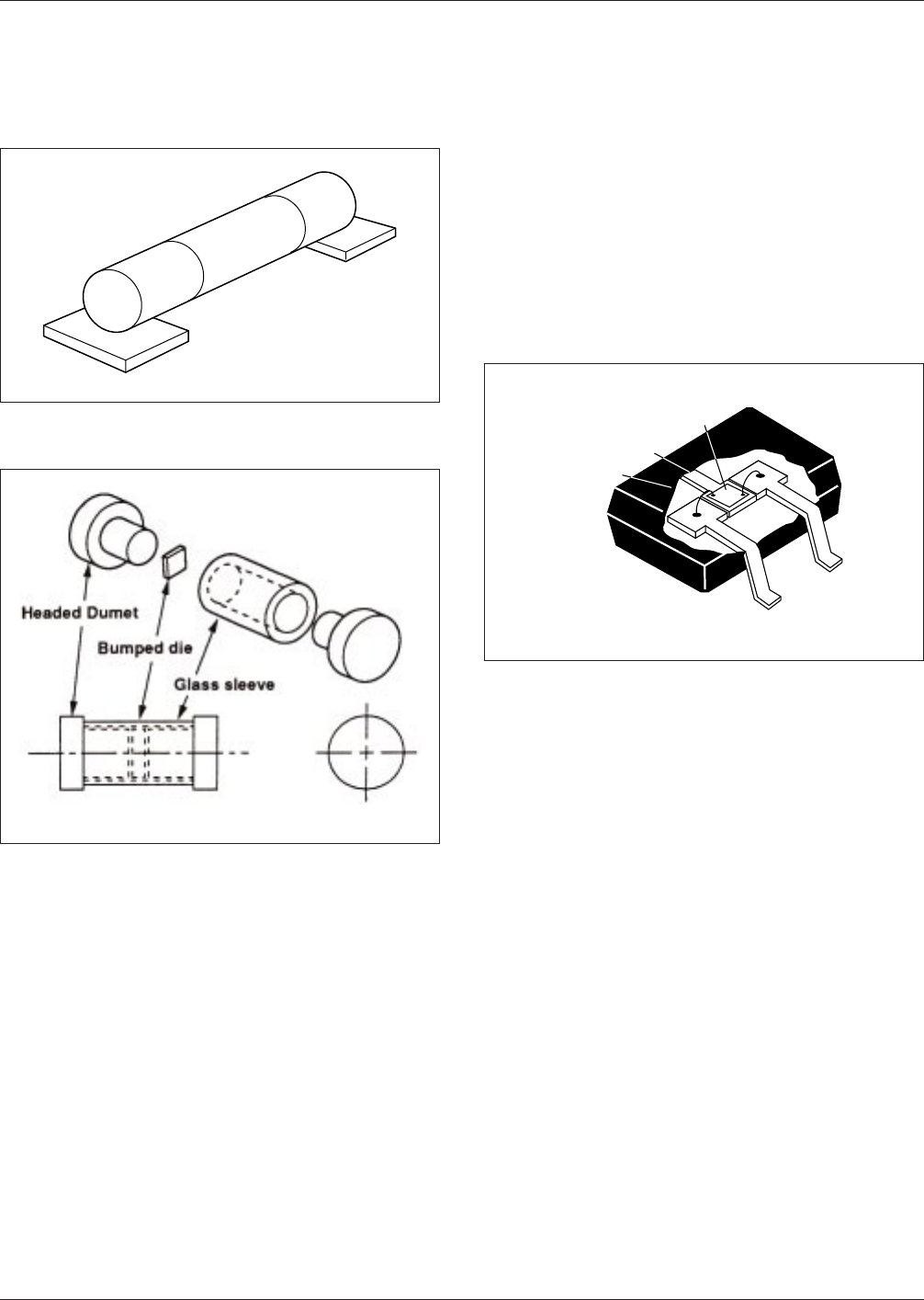
8.5.1 Basic Construction See Figures 8-6 and 8-7.
8.5.2 Marking Parts are available with or without
marked values.
8.5.3 Carrier Package Format Bulk rods, 8 mm tape/4
mm pitch is preferred for best handling. Tape and reel
specifications provide additional requirements.
8.5.4 Resistance to Soldering Parts should be capable
of withstanding five cycles through a standard reflow sys-
tem operating at 215 °C [419 °F]. Each cycle shall consist
of 60 seconds exposure at 215 °C [419 °F]. Parts must also
be capable of withstanding a minimum of 10 seconds
immersion in molten solder at 260 °C [500 °F]. See IPC/
JEDEC J-STD-020 for appropriate reflow cycles and pro-
files when using lead free solders.
8.6 SOT23 One of the first active devices in packaged
form for surface mounting was the SOT device. Plastic
encapsulated three terminal devices with leads formed out
from the body were surface mounted to overcome some of
the problems and difficulties in handling dip transistors. In
general, SOT packages are used with diodes, transistors,
and small I/O devices. The SOT 23 package is the most
common three-lead surface mount configuration.
8.6.1 Basic Construction The SOT 23 package has had
several redesigns to meet the needs of both hybrid and
printed board surface mount industries. These changes
resulted in low, medium and high profile characteristics
which basically reflect the clearance that the body is from
the mounting surface. See Figure 8-8 for construction char-
acteristics.
8.6.2 Marking Parts are available with or without
marked values.
8.6.3 Carrier Package Format Carrier package format
shall be according to the following: body type TO-236,
8 mm tape/4 mm pitch.
8.6.4 Resistance to Soldering Parts should be capable
of withstanding five cycles through a standard reflow sys-
tem operating at 215 °C [419 °F]. Each cycle shall consist
of 60 seconds exposure at 215 °C [419 °F]. Parts must also
be capable of withstanding a minimum of 10 seconds
immersion in molten solder at 260 °C [500 °F]. See IPC/
JEDEC J-STD-020 for appropriate reflow cycles and pro-
files when using lead free solders.
8.7 SOT89 These parts are for high power transistors and
diodes. These parts are used where heat transfer to a sup-
porting structure is important. IPC-7352 SOT89 component
outlines are derived from outline TO-243 Issue ‘‘C’’ within
JEDEC Publication 95.
8.7.1 Basic Construction See Figure 8-9. The SOT 89
package dimensions are designed to meet the needs of both
the hybrid and printed board surface mount industries. In
IPC-7351-8-06
Figure 8-6 Metal Electrode Face Component
Construction
IPC-7351-8-07
Figure 8-7 Break-Away Diagram of MELF Components
IPC-7351-8-08
Figure 8-8 SOT 23 Construction
Passivated
Semiconductor Chip
Collector Lead
Bonding Wire
Epoxy Body
Emitter
Lead
Base
Lead
February 2005 IPC-7351
47