IPC-7351-2005_表面贴装焊盘布局设计和标准通用要求.pdf - 第70页
14.2.2.3 Thermally Enhanced Matrix A thermally enhanced matrix is a perimeter matrix with contacts added back in the center (see Figure 14-6). 14.2.2.4 Staggered Matrix A staggered matrix is defined by the removal of ever…
electrical performance and will increase the overall pack-
age profile. Also the columns are not as rugged as ball
contact and are susceptible to handling damage.
14.2 General Configuration Issues
14.2.1 Device Outlines
The Grid Array package outlines
detailed in this document are furnished in JEDEC Publica-
tion JEP95. The overall outline specification for the array
device allows a great deal of flexibility as far as lead pitch,
contact matrix pattern and construction. The JEDEC stan-
dards allow for die attachment on either side of the inter-
face structure (cavity up or cavity down). Refer to IPC-
7096 for further definition and interconnect schemes for
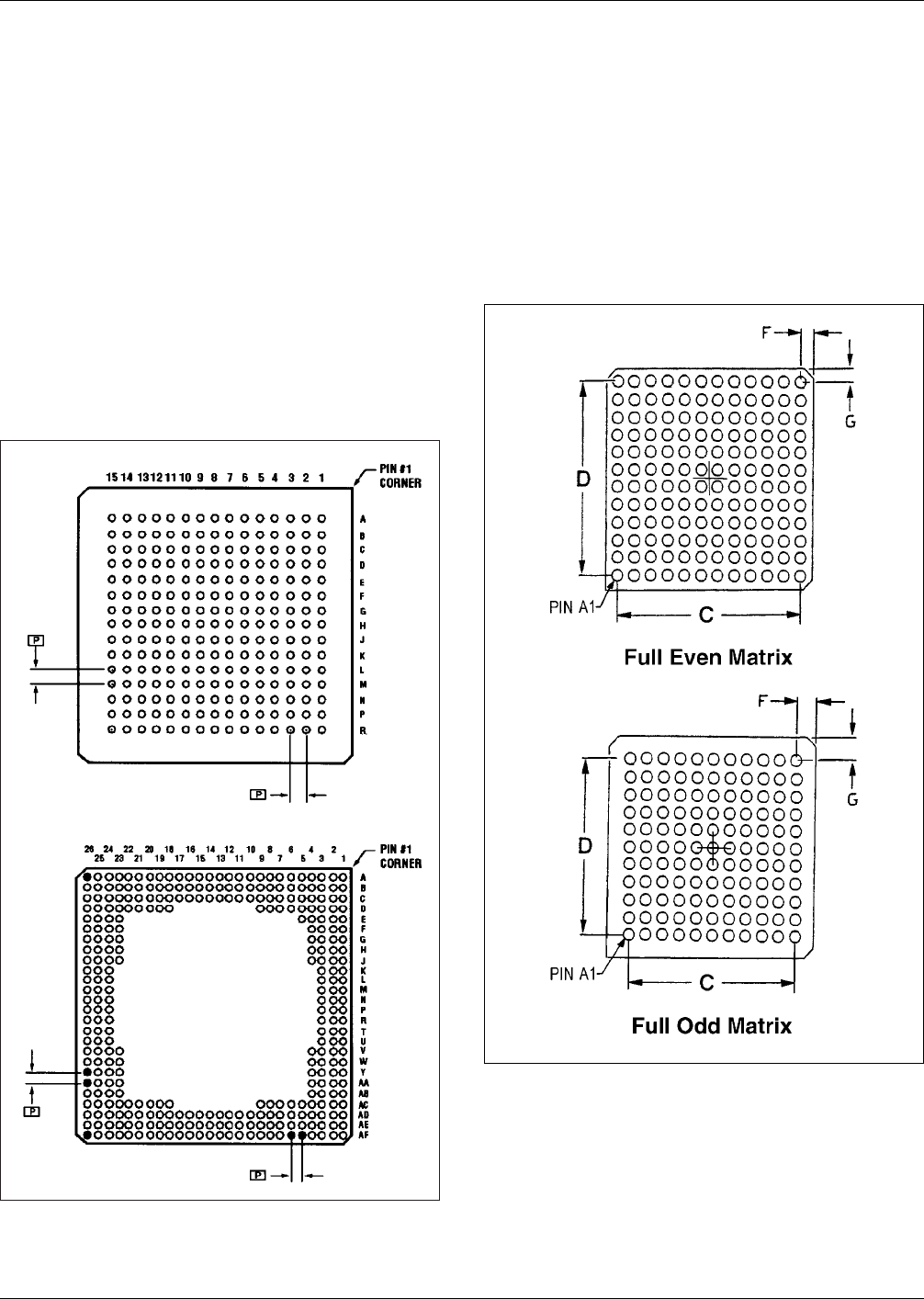
BGAs. The example shown in Figure 14-4 illustrates two
225 I/O devices with a common package outline but, with
the variation of contact pitch, a unique matrix format is
provided.
14.2.2 Contact Matrix Options Contacts may be distrib-
uted in a uniform pattern, however the matrix is always
centered about the centerline of the package (see Figure
14-5). Contact depopulation is permitted at the discretion
of the device manufacturer. Contact patterns can usually be
described in the following methods: full even matrix, full
odd matrix, perimeter matrix, or staggered matrix.
14.2.2.1 Full Matrix For a given package size, there are
two full matrix possibilities: even and odd. One of them is
the largest matrix that theoretically could fit on the pack-
age, given the size and pitch of the contacts. The other
matrix is smaller by one row and column (see Figure 14-5).
14.2.2.2 Perimeter Matrix A perimeter matrix is
achieved by removing an array of contacts from the center
of the matrix. Center-depopulation does not affect the cen-
terline of the matrix (see Figure 14-6). In addition, Perim-
eter matrices are usually described by the number of con-
tact perimeters.
IPC-7351-14-04
Figure 14-4 Bottom View of BGA Devices
IPC-7351-14-05
Figure 14-5 One Package Size, Two Full Matrices
February 2005 IPC-7351
59
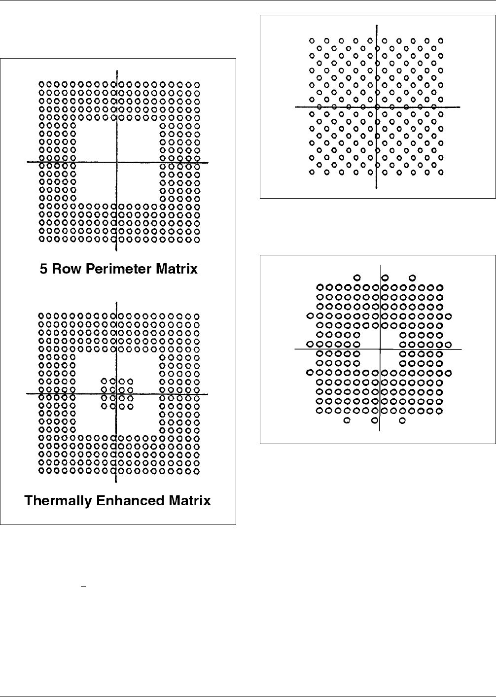
14.2.2.3 Thermally Enhanced Matrix A thermally
enhanced matrix is a perimeter matrix with contacts added
back in the center (see Figure 14-6).
14.2.2.4 Staggered Matrix A staggered matrix is defined
by the removal of every other contact in an interstitial pat-
tern. This provides an effective minimum center-to-center
contact spacing of
√
2 x pitch of the full matrix (see Figure
14-7). In order to retain the A1 contact position, the stag-
gered matrix must be developed using a full odd matrix.
14.2.3 Selective Depopulation In addition to depopula-
tion methods which lead to the matrices described above,
contacts may be removed selectively. Selective depopula-
tion can be accomplished in any manner as long as the pat-
tern matrix is not shifted from the center of the package
outline (see Figure 14-8).
14.2.4 Attachment Site Planning The attachment site or
land pattern geometry recommended for BGA devices is
round with the diameter adjusted to meet contact pitch and
size variation. The diameter of the land should be no larger
than the diameter of the land at the package interface and
is typically 20% smaller than the normal diameter specified
for the ball contact for pitches greater than 1.0 mm and
10% smaller for pitches less than 1.0 mm. Refer to the
manufacturer specification before finalizing land pattern
array and geometry.
14.2.4.1 Copper Defined Land Pattern The land pat-
terns described are defined by the etched copper. Solder
mask clearance should be a minimum of 0.075 mm
[0.00295 in] from the etched copper land. For applications
requiring a clearance that is less than recommended, con-
sult with the printed board supplier.
IPC-7351-14-06
Figure 14-6 Perimeter and Thermally Enhanced Matrices
IPC-7351-14-07
Figure 14-7 Staggered Matrix
IPC-7351-14-08
Figure 14-8 Selective Depopulation
IPC-7351 February 2005
60
标准分享网 www.bzfxw.com 免费下载
14.2.4.2 Solder Mask Defined Land Pattern If solder
mask defined patterns are used, then adjust land pattern
diameter accordingly (see 14.4).
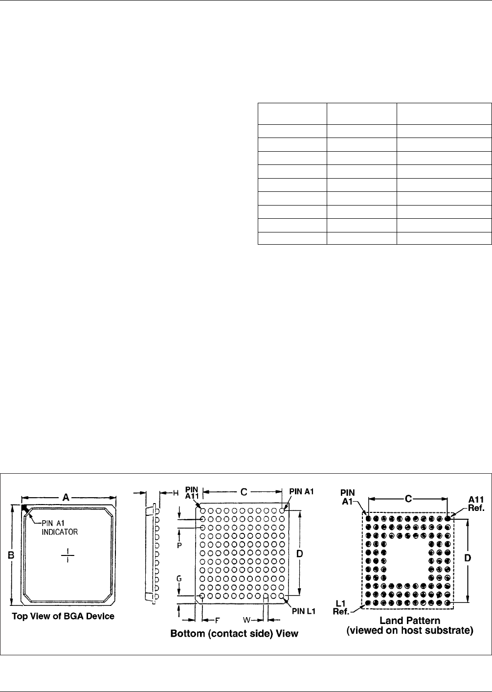
14.2.5 Defining Contact Assignment Array contact
identification is assigned by the column and row location.
For example, A1 contact position is always at an outside
corner position with alpha characters arranged in a vertical
(row) pattern from top to bottom. Numeric characters are
assigned in a horizontal (column) axis (I, O, Q, S, X and Z
are omitted) (see Figure 14-9).
The designer should note that the A1 position is at the
upper left hand corner when the device is viewed from the
top. Contact pattern is defined when viewed from the bot-
tom. The land pattern provided on the host substrate is
opposite of the contact pattern (with A1 contact position
again at the upper left).
14.3 Handling and Shipping For information on trays
and shipping containers refer to ACH:EIA-481-A,
ACH:EIA-481-3, JEDEC CO-028, and JEDEC CO-029.
14.4 Land Pattern Analysis The following provides an
analysis of tolerance assumptions and result in solder joints
based on the land pattern dimensions shown in Figure 14-9.
The variations that exist in determining these land patterns
include the diameter of the individual ball, the positional
accuracy of the ball in relationship to a true position on the
component and the board, and the manufacturing allow-
ance that can be held for the land on the substrate that
mounts the particular ball. The land pattern of the compo-
nent (where the ball is attached) and the land pattern of the
substrate mounting structure (printed board) should be as
similar as possible. Component manufacturers have made
their determinations that the land pattern of pad on the
component should be less than the ball diameter. They base
their conclusions on the resulting nominal ball diameter
with a slight reduction in the land approximation. Pitch
plays a large role in the determination of what ball diam-
eters can be used in various combinations. Table 14-2
shows the characteristics of those balls that are used with
pitches of 1.5 mm through 1.0 mm, as well as future ball
sizes whose pitches fall between 0.40 mm and 0.25 mm.
14.4.1 Land Approximation In each instance, component
manufacturers and board designers are encouraged to
reduce the land size by some percentage of the nominal
ball diameter. The amount of reduction is based on the
original ball size, which is used to determine the average
land. In determining the relationship between nominal
characteristics, a manufacturing allowance for land size has
been determined to be 0.1 mm between the Maximum
Material Condition (MMC) and Least Material Condition
(LMC). Table 14-3 shows the reduction characteristics, the
nominal land size, and the target land dimensions, as well
as future approximations for ball diameters of 0.25 mm and
below.
14.4.2 Total Variation The total variation of the system
considers three major issues: positioning, ball tolerance,
and substrate tolerance. All three attributes added together
IPC-7351-14-09
Figure 14-9 Device Orientation and Contact A1 Position
Table 14-2 Ball Diameter Sizes (mm)
Nominal Ball
Diameter Total Variation Pitch
0.75 0.90 - 0.65 1.5, 1.27
0.60 0.70 - 0.50 1.0
0.50 0.55 - 0.45 1.0, 0.80
0.45 0.50 - 0.40 1.0, 0.80, 0.75
0.40 0.45 - 0.35 0.80, 0.75, 0.65
0.30 0.35 - 0.25 0.80, 0.75, 0.65, 0.50
0.25 0.28 - 0.22 0.40
0.20 0.22 - 0.18 0.30
0.15 0.17 - 0.13 0.25
February 2005 IPC-7351
61