IPC-7351-2005_表面贴装焊盘布局设计和标准通用要求.pdf - 第37页
www.bzfxw.com 3.4.6.5 Vias as Test Points V ia holes, in addition to being used for connecting surface mounted component lands to conductor layers, may also be used as test targets for bed-of-nails type probes and/or rew…
www.bzfxw.com
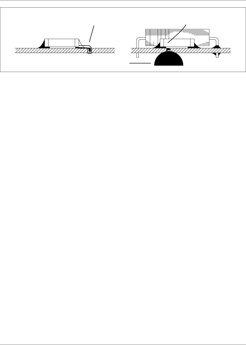
3.4.6.3 Vias Under Components During wave soldering
of the assembly, flux may potentially become trapped
under zero clearance devices. If the assembly is to be wave
soldered, via holes underneath zero clearance components
on the primary side should be avoided on boards unless
vias are tented with soldermask. Untented via holes may be
located underneath zero clearance surface mount packages
in reflow soldered surface mount assemblies that will not
be exposed to wave soldering (see Figure 3-16).
3.4.6.4 Vias Within Lands Via holes within the surface
mount component attachment lands are permitted only if
the via is plated closed, filled or plugged and capped
(plated) in such a way as to prevent solder migration dur-
ing the component attachment process. A blind or plated
closed micro-via in the land is typically acceptable for sol-
der attachment of surface mount components. Refer to
IPC-2226 for minimum annular ring requirements for
microvias.
IPC-7351-3-14
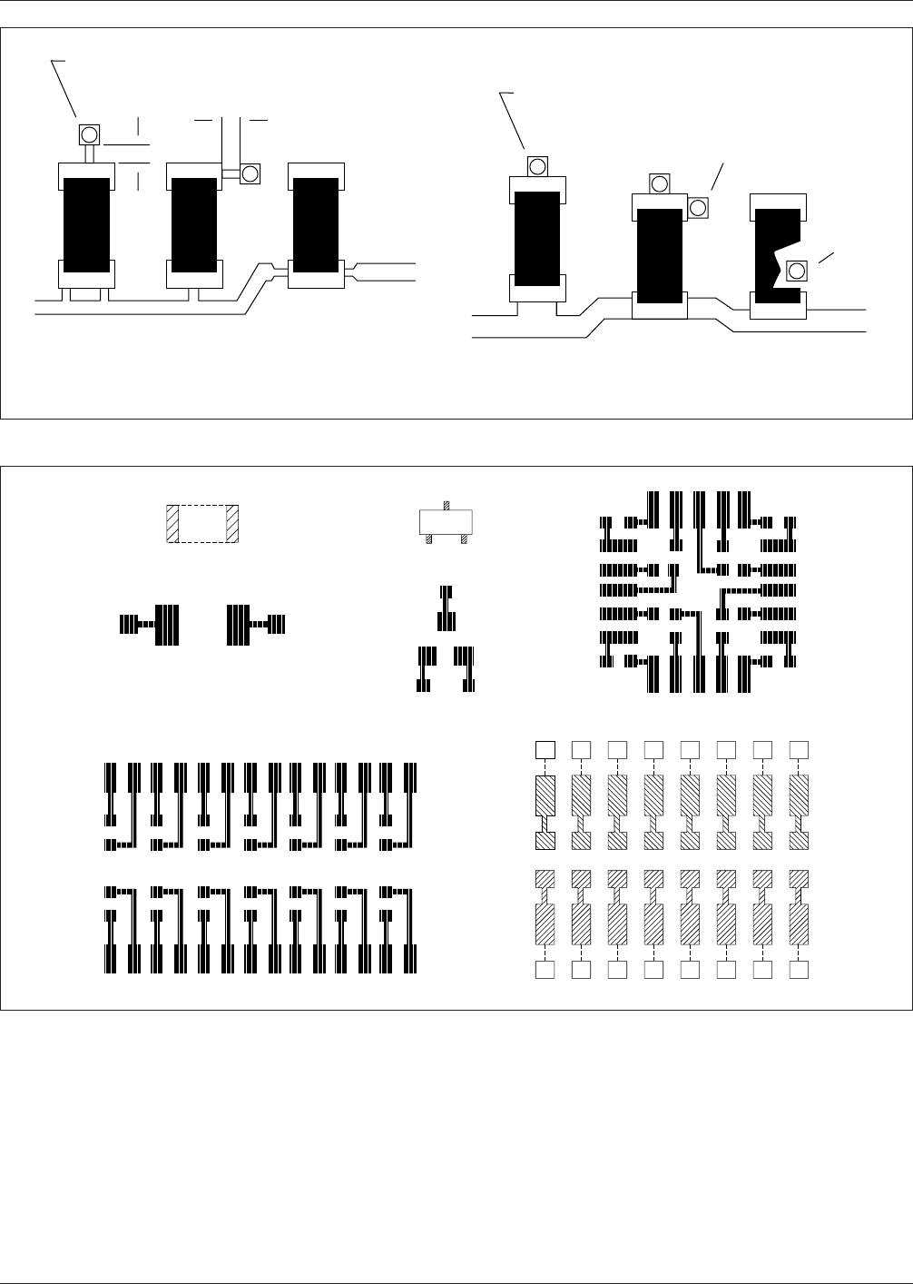
Figure 3-14 Land Pattern to Via Relationship
▼
▼
▼
▼
▼
Square land
0.50 mm
[0.020 in] min
Chip Components and Feed Through Via Holes
0.50 mm
[0.020 in] min
Good Design
Poor Design
Feed through lands flush against contact area
▼
▼
▼
Too close
to contact
area
IPC-7351-3-15
Figure 3-15 Examples of Via Positioning Concepts
Side 2
Vias
Side 1
Vias
Side 1
Vias
Side 2
Vias
Chip Component
Chip Component
PLCC
SOIC
SOIC
IPC-7351 February 2005
26
标准分享网 www.bzfxw.com 免费下载
www.bzfxw.com
3.4.6.5 Vias as Test Points Via holes, in addition to
being used for connecting surface mounted component
lands to conductor layers, may also be used as test targets
for bed-of-nails type probes and/or rework ports. When a
via is used as a test point it is required that the x-y location
and size of a test land be defined as a secondary file for test
fixture development.
3.4.7 Standard PCB Fabrication Allowances Manufac-
turing tolerances or standard fabrication allowances (SFA)
exist in all PCB fabrication shops. Virtually every registra-
tion or alignment operation that is performed has some
potential for misregistration. There are approximately 42
basic steps in fabricating a multilayer PCB, several of
which involve operations that require precision in location
and alignment. The tolerance varies according to the
printed board maximum diagonal dimension and must be
included in the land size calculations. The fabricator should
be consulted prior to beginning a design to determine their
SFA. With this SFA value, the designer can proceed
accordingly, preventing tolerances from stacking up and
creating yield and/or production problems.
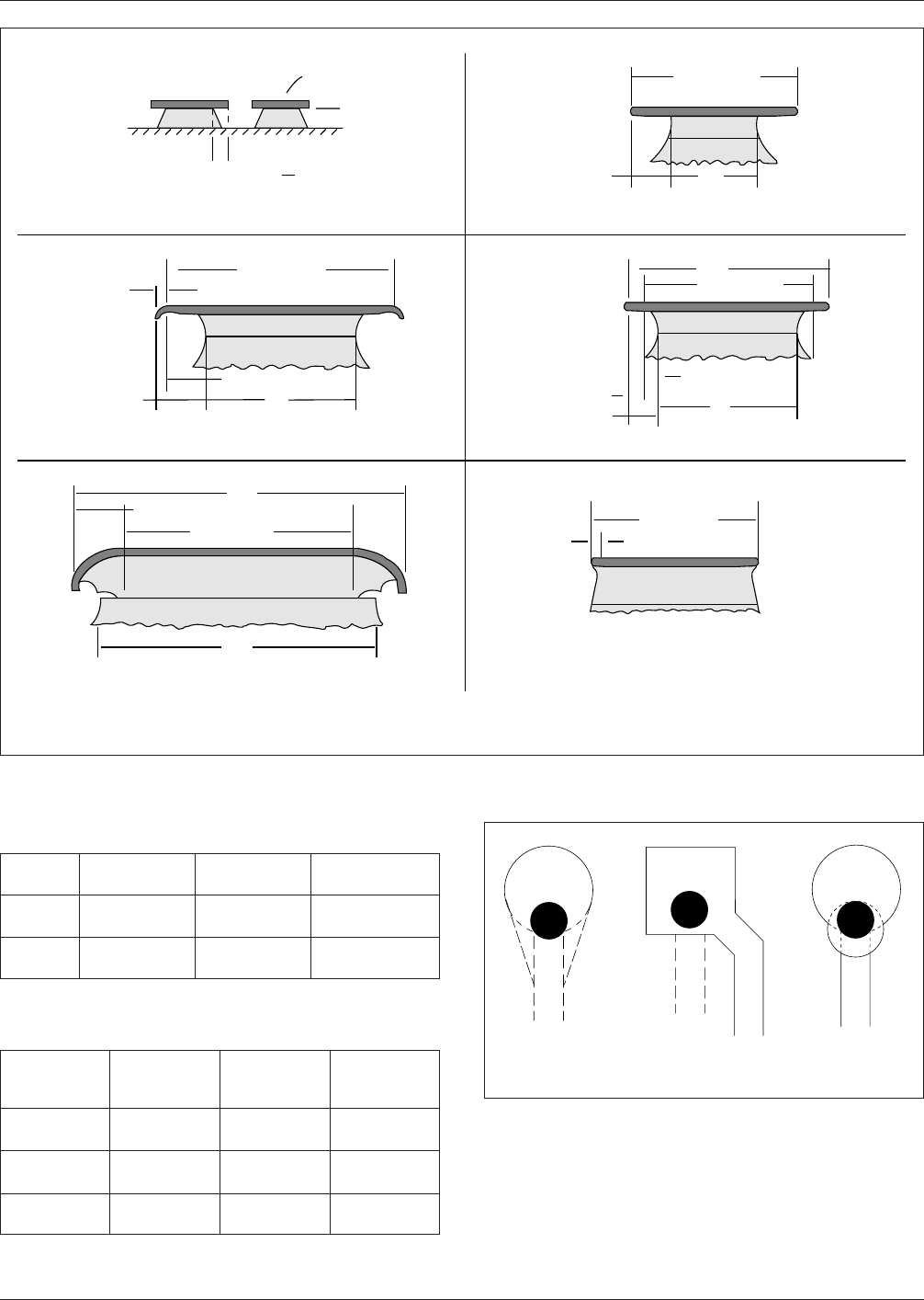
3.4.7.1 PCB Manufacturing Characteristics Figure
3-17 shows the various characteristics of conductor geom-
etry after etching. End-product drawings and specifications
should specify only the minimum for conductor spacing;
however, conductor widths should be defined according to
minimum values, where land patterns should be defined as
to their maximum material conditions (MMC). Clear target
values for conductors and land patterns will help the manu-
facturer achieve the desired condition.
3.4.7.2 Conductor Width Tolerances Table 3-17 repre-
sents process tolerances that can be expected with normal
processing. (Specific process tolerances should be dis-
cussed with the board manufacturer.) The bilateral toler-
ances in Table 3-17 are typical for 0.046 mm [0.00181 in]
copper. For additional copper thickness, a further width
variation can be expected (see Figure 3-17).
3.4.7.3 Conductive Pattern Feature Location Toler-
ance
Table 3-18 is for the tolerance to be applied to the
nominal dimension chosen for the location of the lands,
connector contacts and conductors in relation to the datum
reference. These tolerances include master pattern accu-
racy, material movement, layer registration and fixturing.
3.4.7.4 Annular Ring Control Annular ring is defined as
the amount of land that remains after a hole is drilled
through it. With high-density SMT designs, maintaining
minimum annular requirements has emerged as one of the
most difficult parts of multilayer PCB fabrication in terms
of producibility. Perfect registration will maximize the
annular ring all around the drilled hole.
For example, using a 0.8 mm [0.0315 in] land with a 0.5
mm [0.0197 in] drill will result in a 0.15 mm [0.00591 in]
annular ring under perfect registration conditions. If mis-
registration of 0.15 mm [0.00591 in] occurs in any direc-
tion, the result will be a 0.3 mm [0.012 in] annular ring on
one side of the pad, and no annular ring on the other side.
If misregistration is greater than 0.15 mm [0.00591 in], i.e.,
0.2 mm [0.0079 in], then the drill will actually break out of
the land. If the breakout is in the direction where the con-
ductor connects to the land, the drill will effectively discon-
nect the conductor from the land. The net result is a
scrapped PCB. Since signal conductors intersect the lands
from all directions, any breakout has the potential to ran-
domly disconnect conductors all over the PCB.
Maintaining consistent annular ring control is difficult, but
methods have been developed to insure connectivity
between lands and conductors. Each method is intended to
provide copper material where the conductor enters the
land. The land which has the added material may resemble
a teardrop or keyhole or adopt alternate designs as shown
in Figure 3-18.
3.4.8 Panelization Components can be mounted on indi-
vidual boards or on boards that are organized in a panel
form. Boards or panels that will be moved by automatic
handling equipment or pass through automated operations
(parts placement, soldering, cleaning, etc.) must have spe-
cific areas kept free of parts or active circuitry. Typically, a
clear area of 3.0 mm [0.012 in] to 5.0 mm [0.0197 in] wide
must be allowed along the sides for the clearance. The
required clearance width is dependent upon the design of
IPC-7351-3-16
Figure 3-16 Vias Under Components
Caution
Solder
Characteristic
Solder
Migration
▼
▼
Wave Solder
▼
February 2005 IPC-7351
27
www.bzfxw.com
IPC-7351-3-17
Figure 3-17 Conductor Description
▼
LaminateX
▼
Etch Factor =
V
X
An etch factor of 1/1 is usually considered practical.
Higher factors may be specified for some applications.
Resist
▼
V
▼
▼
"B" (DCW)
"E" Outgrowth
▼
▼
▼
▼
▼
▼
▼
"C" Undercut
▼
"A"
(MCW)*
Overhang
Panel Plating (Liquid Resist)
▼
▼
(OCW)*
▼
▼
"D"
"B" (DCW)*
"E" Outgrowth
▼
▼
(MCW)*
"A"
▼
▼
Pattern Plating (Liquid Resist)
▼
"B" (DCW)
(MCW)*
"C" Undercut
& Overhang
Panel Plating (Dry Film Resist)
▼
▼
"A"
▼
▼
▼
▼
▼
"D"
▼
"A"
(MCW)*
Overhang
Pattern Plating (Dry Film Resist)
▼
▼
▼
(OCW)*
"B" (DCW)*
▼
▼
▼
▼
"E" Outgrowth
▼
▼
"C" Undercut
▼
▼
"B" (DCW)*
▼
"C" Undercut
▼
Thin Clad & Pattern Plating (Dry Film Resist)
A = MCW (Minimum Conductor Width) B = DCW (Design Conductor Width) D = OCW (Overall Conductor Width)
Table 3-17 Conductor Width Tolerances,
0.046 mm [0.00181 in] Copper, mm [in]
Feature
Producibility
Level A
Producibility
Level B
Producibility
Level C
Without
plating
± 0.06 mm
[± 0.00236 in]
± 0.04 mm
[± 0.00157 in]
± 0.015 mm
[± 0.0005906 in]
With
plating
± 0.10 mm
[± 0.00393 in]
± 0.08 mm
[± 0.00314 in]
± 0.05 mm
[± 0.0197 in]
Table 3-18 Feature Location Accuracy (units: mm [in])
Greatest
Board/ X,Y
Dimension
Producibility
Level A
Producibility
Level B
Producibility
Level C
Up to 300
[11.81]
0.30
[0.012]
0.20
[0.00787]
0.10
[0.00394]
Up to 450
[17.72]
0.35
[0.0138]
0.25
[0.00984]
0.15
[0.00591]
Up to 600
[23.62]
0.40
[0.0157]
0.30
[0.012]
0.20
[0.00787]
IPC-7351-3-18
Figure 3-18 Examples of Modified Landscapes
Corner Entry
Filleting
Key Holing
IPC-7351 February 2005
28
标准分享网 www.bzfxw.com 免费下载