IPC-7351-2005_表面贴装焊盘布局设计和标准通用要求.pdf - 第26页
www.bzfxw.com Additional suf f ixes for alternate components that do not follow JEDEC, EIA or IEC standards are as follows: ‘ ‘A ’ ’ – Alternate Component (used for SOP and QFP when component tolerance or height is dif f…
www.bzfxw.com
Sometimes a dimension is presented as a minimum dis-
tance. This occurs when defining a space(s) that exists
between lands at MMC. The printed board manufacturer
may not always inspect the board in accordance with the
limit concepts shown in the table. However, these limits
may be used as the criteria for go/no-go acceptance of the
printed board land pattern. The dimensions shown in each
table are those that have been used in the equations
described in 3.1 for determining the recommended land
patterns. The maximum material condition for each land
pattern analysis level describes the most robust joint or
land protrusion for that level land pattern.
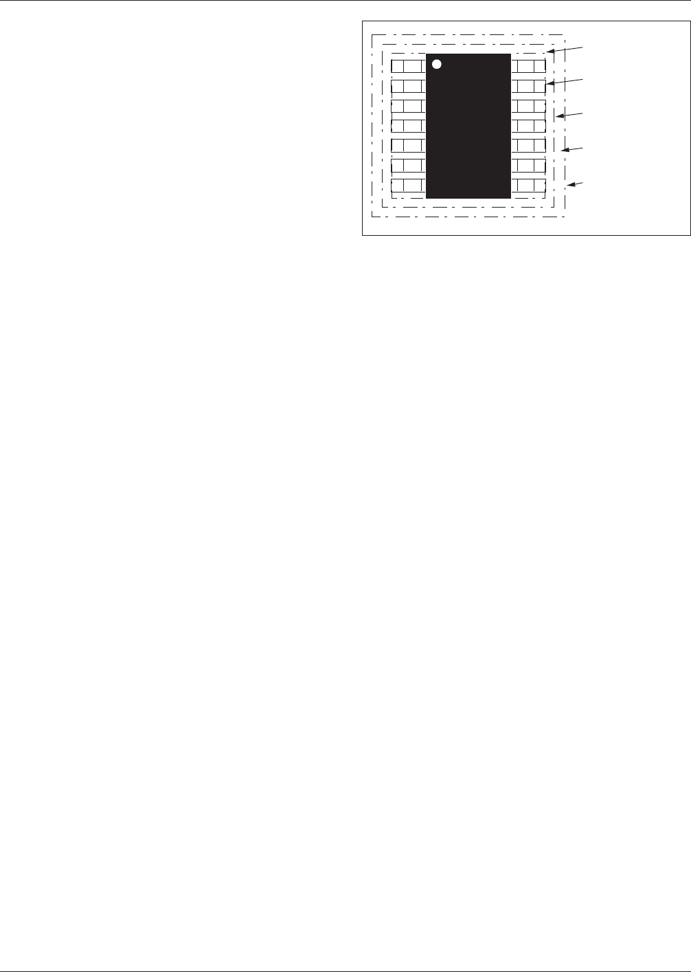
3.1.5.4 Courtyard Determination The courtyard of any
land pattern is the smallest area that provides a minimum
electrical and mechanical clearance of both the component
maximum boundary extremities and/or the land pattern
maximum boundary extremities. The intent of the court-
yard is to aid the designer in determining the minimum
area occupied by the combination of component and land
pattern. The information provided in Tables 3-2 through
3-14 is intended to relate to those excesses that should be
added to the maximum dimension to derive the appropriate
courtyard condition.
As an example, if a component was the major determining
factor of the boundary condition, it would have the excess
added to the dimensions. The same holds true for a land
pattern that has the greater extremities. If either dimension
were 14.5 mm, and the excess from tables 3-2 through 3-14
indicated an excess of 0.8 mm, the resulting courtyard
would theoretically be 16.1 mm. The tables further define
a round-up feature. If the round-up were recommended as
being to the nearest 0.5 mm, the courtyard would become
16.5 mm.
It should be noted that 16.5 mm is a number that, when
divided by 2 to obtain the component centroid, provides 2
decimal places to the right of the number. It therefore may
be appropriate to keep this number in an even approxima-
tion such as 16.6 mm. This would provide 8.3 mm to either
side of the center of the component to help designers posi-
tion the component in relation to some grid or placement
algorithm.
When manufacturing allowance must be considered in the
design process the courtyard represents the starting point of
the minimum area needed for the component and the land
pattern. Manufacturing, assembly and testing representa-
tives should assist in determining the additional room
needed to accommodate placement, testing, modification
and repair. This manufacturing allowance is usually depen-
dent on the density and complexity of the product, and is
not defined in this document. The manufacturing allowance
is determined by application and manufacturing process
requirements (see Figure 3-5).
3.1.5.5 Land Pattern Naming Convention The RLP
(Registered Land Pattern) numbering scheme previously
used in IPC-SM-782A has been replaced with an intelligent
land pattern naming convention which will aid in the stan-
dardization of electronic schematic symbols for engineer-
ing.
Each land pattern in the IPC-7351 has received a name
containing a prefix for the device type, a pin pitch, a nomi-
nal lead span corresponding to the ‘‘L’’ dimension (or a
pair of nominal lead spans for components with termina-
tion leads on four sides), and a pin quantity. In the case of
ball grid array (BGA) packages, the column and row num-
bers are given as there are no end termination lead spans.
The purpose of the number is to aid in communication
between engineering, design, and manufacturing. Specific
syntax explanations include:
The + (plus sign) stands for ‘‘in addition to’’ (no space
between the prefix and the body size).
The - (dash) is used to separate the pin qty.
The X (capital letter X) is used instead of the word ‘‘by’’
to separate two numbers such as height X width like
‘‘Quad Packages.’’
The suffix letters of L, M and N are reserved by IPC. The
suffix letters ‘‘L,’’ ‘‘M,’’ and ‘‘N’’ have been reserved to
signify when the land protrusion is at their minimum
(least), maximum (most), or median (nominal) protrusion
or use environment as follows:
M – Maximum (Most) Material Condition
(Density Level A)
N – Median (Nominal) Material Condition
(Density Level B)
L – Minimum (Least) Material Condition
(Density Level C)
Note: Ball Grid Array (BGA) and Quad Flat No-Lead
(QFN) packages do not receive a suffix of ‘‘L,’’ ‘‘M’’ or
‘‘N’’ as they are only listed in the median (nominal) den-
sity level.
IPC-7351-3-05
Figure 3-5 Courtyard Boundary Area Condition
Component / Pattern
(Maximum Boundary)
Courtyard
Excess
Courtyard
(Minimum Area)
Manufacturing
Allowance
Courtyard
Manufacturing Zone
February 2005 IPC-7351
15

www.bzfxw.com
Additional suffixes for alternate components that do not
follow JEDEC, EIA or IEC standards are as follows:
‘‘A’’ – Alternate Component (used for SOP and QFP
when component tolerance or height is different)
‘‘B’’ – Second Alternate Component
Additional suffices for JEDEC and EIA Standard parts that
have several alternate packages are as follows:
AA, AB, AC JEDEC or EIA Component Identifier (Used
primarily on Chip Resistors, Inductors and Capacitors).
The naming conventions shown in Table 3-15 are subject to
change as new component families are identified. The most
current naming convention listing can be found on the IPC
website (www.ipc.org) under ‘‘PCB Tools and Calcula-
tors.’’.
Table 3-15 IPC-7351 Land Pattern Naming Convention
COMPONENT, CATEGORY LAND PATTERN NAME
Ball Grid Array’s, Inch Based (1.27 mm / 0.05 in Pitch) ........ BGA127P + Number of Pin Columns X Number of Pin Rows - Pin Qty
Ball Grid Array’s, Metric Based (1.50 mm Pitch) ................... BGA150P + Number of Pin Columns X Number of Pin Rows - Pin Qty
Ball Grid Array’s, Metric Based (1.00 mm Pitch) ................... BGA100P + Number of Pin Columns X Number of Pin Rows - Pin Qty
Ball Grid Array’s, Metric Based (0.80 mm Pitch) ..................... BGA80P + Number of Pin Columns X Number of Pin Rows - Pin Qty
Ball Grid Array’s, Metric Based (0.75 mm Pitch) ..................... BGA75P + Number of Pin Columns X Number of Pin Rows - Pin Qty
Ball Grid Array’s, Metric Based (0.65 mm Pitch) ..................... BGA65P + Number of Pin Columns X Number of Pin Rows - Pin Qty
Ball Grid Array’s, Metric Based (0.50 mm Pitch) ..................... BGA50P + Number of Pin Columns X Number of Pin Rows - Pin Qty
Ball Grid Array’s w/Staggered Pins (1.27 mm Pitch) ........... SBGA127P + Number of Pin Columns X Number of Pin Rows - Pin Qty
Capacitors, Chip, Array ................................................................ CAPCA + Pitch P + Body Width X Body Length in Metric - Pin Qty
Capacitors, Chip, Polarized .................................................................................................................... CAPCP + Body Size in Metric
Capacitors, Chip, Nonpolarized ................................................................................................................ CAPC + Body Size in Metric
Capacitors, Chip, Wire Rectangle ...................................................................................................... CAPCWR + Body Size in Metric
Capacitors, Molded, Nonpolarized ........................................................................................................... CAPM + Body Size in Metric
Capacitors, Molded, Polarized ............................................................................................................... CAPMP + Body Size in Metric
Capacitors, Aluminum Electrolytic ................................................................................... CAPAE + Base Body Width (W) + Height (H)
Ceramic Flat Packages ....................................................................................................... CFP127P + Lead Span Nominal - Pin Qty
Column Grid Array’s ........................................................................ CGA + Number of Pin Columns X Number of Pin Rows - Pin Qty
Diodes, Molded (JEDEC Standard Package) ........................................................................................... DIOM + Body Size in Metric
Diodes, MELF ..................................................................................................................................... DIOMELF + Body Size in Metric
Inductors, Chip ........................................................................................................................................... INDC + Body Size in Metric
Inductors, Chip, Array .................................................................... INDCA + Pitch P + Body Width X Body Length in Metric - Pin Qty
Inductors, Molded ...................................................................................................................................... INDM + Body Size in Metric
Inductors, Precision Wire Wound ............................................................................................................... INDP + Body Size in Metric
Plastic Leaded Chip Carriers Square (JEDEC Standard Package) ............................................................................. PLCC - Pin Qty
Plastic Leaded Chip Carriers Rectangular (JEDEC Standard Package) .................................................................. PLCCR - Pin Qty
Plastic Leaded Chip Carrier Sockets Square ............................................................................................................ PLCCS - Pin Qty
Plastic Leaded Chip Carrier Sockets Rectangular .................................................................................................. PLCCRS - Pin Qty
Plastic Quad Flat Packages, 0.635 mm Pitch, Pin 1 Side ........................................................................................ PQFPS - Pin Qty
Plastic Quad Flat Packages, 0.635 mm Pitch, Pin 1 Center ..................................................................................... PQFPC - Pin Qty
Bumper Quad Flat Packages, 0.635 mm Pitch, Pin 1 Side ...................................................................................... BQFPS - Pin Qty
Bumper Quad Flat Packages, 0.635 mm Pitch, Pin 1 Center .................................................................................. BQFPC - Pin Qty
Quad Flat Packages, 1.00 mm Pitch .................................................. QFP100P + Lead Span L1 X Lead Span L2 Nominal - Pin Qty
Quad Flat Packages, 0.80 mm Pitch .................................................... QFP80P + Lead Span L1 X Lead Span L2 Nominal - Pin Qty
Quad Flat Packages, 0.65 mm Pitch .................................................... QFP65P + Lead Span L1 X Lead Span L2 Nominal - Pin Qty
Shrink Quad Flat Packages, 0.50 mm Pitch ...................................... SQFP50P + Lead Span L1 X Lead Span L2 Nominal - Pin Qty
Shrink Quad Flat Packages, 0.40 mm Pitch ...................................... SQFP40P + Lead Span L1 X Lead Span L2 Nominal - Pin Qty
Shrink Quad Flat Packages, 0.30 mm Pitch ...................................... SQFP30P + Lead Span L1 X Lead Span L2 Nominal - Pin Qty
Thin Quad Flat Packages, 0.80 mm Pitch, Height ≤ 1.60 mm .......... TQFP80P + Lead Span L1 X Lead Span L2 Nominal - Pin Qty
Thin Quad Flat Packages, 0.65 mm Pitch, Height ≤ 1.60 mm .......... TQFP65P + Lead Span L1 X Lead Span L2 Nominal - Pin Qty
IPC-7351 February 2005
16
标准分享网 www.bzfxw.com 免费下载

www.bzfxw.com
COMPONENT, CATEGORY LAND PATTERN NAME
Thin Quad Flat Packages, 0.50 mm Pitch, Height ≤ 1.60 mm ........ TSQFP50P + Lead Span L1 X Lead Span L2 Nominal - Pin Qty
Thin Quad Flat Packages, 0.40 mm Pitch, Height ≤ 1.60 mm ........ TSQFP40P + Lead Span L1 X Lead Span L2 Nominal - Pin Qty
Thin Quad Flat Packages, 0.30 mm Pitch, Height ≤ 1.60 mm ........ TSQFP30P + Lead Span L1 X Lead Span L2 Nominal - Pin Qty
Ceramic Quad Flat Packages, 1.27 mm Pitch ................................. CQFP127P + Lead Span L1 X Lead Span L2 Nominal - Pin Qty
Ceramic Quad Flat Packages, 0.80 mm Pitch ................................... CQFP80P + Lead Span L1 X Lead Span L2 Nominal - Pin Qty
Ceramic Quad Flat Packages, 0.635 mm Pitch ................................. CQFP63P + Lead Span L1 X Lead Span L2 Nominal - Pin Qty
Quad Flat No Lead Packages 0.80 mm Pitch ................... QFN80P - Body Width X Body Length in Metric - Pin Qty + Thermal Pad
Quad Flat No Lead Packages 0.65 mm Pitch ................... QFN65P - Body Width X Body Length in Metric - Pin Qty + Thermal Pad
Quad Flat No Lead Packages 0.50 mm Pitch ................... QFN50P - Body Width X Body Length in Metric - Pin Qty + Thermal Pad
Quad Flat No Lead Packages 0.40 mm Pitch ................... QFN40P - Body Width X Body Length in Metric - Pin Qty + Thermal Pad
Quad Leadless Ceramic Chip Carriers (JEDEC Standard Package) .............. LCC + Body Width X Body Length in Metric - Pin Qty
Quad Leadless Ceramic Chip Carriers (Pin 1 on Side) ................................. LCCS + Body Width X Body Length in Metric - Pin Qty
Quad Bottom Chip Carrier (JEDEC MO-217B) ............................................. QBCC + Body Width X Body Length in Metric - Pin Qty
Resistors, Chip ......................................................................................................................................... RESC + Body Size in Metric
Resistors, Chip, Array .................................................................. RESCA + Pitch P + Body Width X Body Length in Metric - Pin Qty
Resistors, Molded ..................................................................................................................................... RESM + Body Size in Metric
Resistors, MELF ................................................................................................................................ RESMELF + Body Size in Metric
Small Outline IC, J-Leaded 300, 350, 400, 450 mil Body Width (Pitch 1.27 mm) ............. SOJ127P + Lead Span Nominal - Pin Qty
Small Outline IC, J-Leaded (Pitch 0.65 mm) ........................................................................ SOJ65P + Lead Span Nominal - Pin Qty
Small Outline Integrated Circuit, 1.27 mm Pitch (Standard 50 mil Pitch SOICs) ............. SOIC127P + Lead Span Nominal - Pin Qty
Small Outline Packages, 1.27 mm Pitch (Nonstandard 50 mil Pitch SOICs) .................... SOP127P + Lead Span Nominal - Pin Qty
Small Outline Packages, 1.00 mm Pitch ............................................................................ SOP100P + Lead Span Nominal - Pin Qty
Small Outline Packages, 0.80 mm Pitch .............................................................................. SOP80P + Lead Span Nominal - Pin Qty
Small Outline Packages, 0.65 mm Pitch .............................................................................. SOP65P + Lead Span Nominal - Pin Qty
Small Outline Packages, 0.635 mm Pitch ............................................................................... SOP63 + Lead Span Nominal - Pin Qty
Shrink Small Outline Packages, 0.50 mm Pitch ................................................................ SSOP50P + Lead Span Nominal - Pin Qty
Shrink Small Outline Packages, 0.40 mm Pitch ................................................................ SSOP40P + Lead Span Nominal - Pin Qty
Shrink Small Outline Packages, 0.30 mm Pitch ................................................................ SSOP30P + Lead Span Nominal - Pin Qty
Thin Small Outline Packages, Height is ≤ 1.60 mm, 1.27 mm Pitch ............................... TSOP127P + Lead Span Nominal - Pin Qty
Thin Small Outline Packages, Height is ≤ 1.60 mm, 1.00 mm Pitch ............................... TSOP100P + Lead Span Nominal - Pin Qty
Thin Small Outline Packages, Height is ≤ 1.60 mm, 0.80 mm Pitch ..................................TSOP80P + Lead Span Nominal - Pin Qty
Thin Small Outline Packages, Height is ≤ 1.60 mm, 0.65 mm Pitch ................................. TSOP65P + Lead Span Nominal - Pin Qty
Thin Shrink Small Outline Packages, Height is ≤ 1.60 mm, 0.55 mm Pitch ................... TSSOP55P + Lead Span Nominal - Pin Qty
Thin Shrink Small Outline Packages, Height is ≤ 1.60 mm, 0.50 mm Pitch ................... TSSOP50P + Lead Span Nominal - Pin Qty
Thin Shrink Small Outline Packages, Height is ≤ 1.60 mm, 0.40 mm Pitch ................... TSSOP40P + Lead Span Nominal - Pin Qty
Thin Shrink Small Outline Packages, Thin (Height is ≤ 1.60 mm) 0.30 mm Pitch .......... TSSOP30P + Lead Span Nominal - Pin Qty
Very Small Outline Packages, 0.762 mm Pitch (0.30 in Pitch) ........................................ VSOP762P + Lead Span Nominal - Pin Qty
SOD (Example: SOD3705 = SOD123) ................................................................................ SOD + Lead Span Nominal + Body Width
SON - Dual No Lead Packages 0.3 - 0.8 mm Pitch .................... SON + Pitch (P) - Body Width X Body Length - Pin Qty + Thermal Pad
SOT89 (JEDEC Standard Package) .......................................................................................................................................... SOT89
SOT143 (JEDEC Standard Package) ...................................................................................................................................... SOT143
SOT343 (JEDEC Standard Package) ...................................................................................................................................... SOT343
SOT143 Reverse (JEDEC Standard Package) ..................................................................................................................... SOT143R
SOT343 Reverse (JEDEC Standard Package) ..................................................................................................................... SOT343R
SOT223 (JEDEC Standard Package) (Example: SOT230P700-4N) ........................ SOT + Pitch (P) + Lead Span Nominal - Pin Qty
SOT Generic Package 0.65 mm Pitch .................................................................................. SOT65P + Lead Span Nominal - Pin Qty
SOT Generic Package 0.95 mm Pitch .................................................................................. SOT95P + Lead Span Nominal - Pin Qty
TO (Generic DPAK) (Example: TO228P970-3N) ...................................................................... TO + Pitch (P) + Lead Span + Pin Qty
February 2005 IPC-7351
17