IPC-7351-2005_表面贴装焊盘布局设计和标准通用要求.pdf - 第69页
electrical performance and will increase the overall pack- age profile. Also the columns are not as rugged as ball contact and are susceptible to handling damage. 14.2 General Configuration Issues 14.2.1 Device Outlines T…
standard reflow system operating within a range of 235 °C
to 260 °C [455 °F to 500 °F] depending on the attachment
alloy being used. Each cycle shall consist of 60 to 90 sec-
onds exposure at the particular temperature selected. See
IPC/JEDEC J-STD-020 for appropriate reflow cycles and
profiles when using lead free solders.
It is important to consider that Plastic BGAs are moisture
sensitive device/components (MSD). Precaution must be
taken during the printed board assembly process in order to
avoid MSD damages (Delamination, Cracks, etc). Trace-
ability for baking PBGA, might be required mainly when
attached in a double sided/reflow printed board assembly.
14.1.2 Fine Pitch BGA Package (FBGA) JEDEC Publica-
tion JEP95, Section 4.5, defines a Fine-pitch Ball Grid
Array (FBGA) package is a reduced-pitch (<1.00 mm) ver-
sion of a Ball-Grid-Array (BGA) package. The carrier body
of the package has a metallized circuit pattern applied to a
dielectric structure. One or more semiconductor devices are
attached to either the top or the bottom surface of this
dielectric carrier. On the underside of the dielectric carrier
is an array pattern of metallized balls, which form the
mechanical and electrical connection from the package
body to a mating feature such as a printed circuit board.
The surface that contains the die may be encapsulated by
various techniques to protect the semiconductor. The
requirements for a square FBGA package family that
allows four optional contact pitch variations; 0.50, 0.65,
0.75 and 0.80 mm and defines four device profile (height)
variations as well. The 0.75 mm pitch has been added to
the list thus providing four pitch variations for FBGA type
parts.
The total profile height of the FBGA, as measured from the
seating plane to the top of the component, is greater than
1.70 mm. The Low-Profile Fine-Pitch Ball-Grid-Array
(LFBGA) and is a reduced-height version of an FBGA.
The total profile height of the LFBGA as measured from
the seating plane to the top of the component, is no greater
than 1.20 mm. Thin-Profile Fine-Pitch Ball-Grid-Array
(TFBGA) is a reduced-height version of an FBGA with a
total profile height as measured from the seating plane to
the top of the component that does not exceed 1.00 mm
and the Very-Thin-Profile Fine-Pitch Ball-Grid-Array
(VFBGA) is a reduced-height version of an FBGA with a
total profile height as measured from the seating plane to
the top of the component that is at or below 0.80 mm.
The JEDEC design guide for FBGA allows the manufac-
turer the option to increase ball diameter as the spacing or
pitch between ball contact centers increase as compared in
Table 14-1. As of this release JEDEC standards do not
support the 0.75 mm pitch, however the industry has some
parts available in that pitch.
The larger ball diameter option has been allowed to accom-
modate packages using rigid interposer structures. The
larger diameter ball may compensate to a degree, for the
wide mismatch of the coefficient of thermal expansion
(CTE) between the silicon die and the rigid PCB structure.
Fine pitch ball parts may require special processing outside
the normal pick/place and reflow manufacturing operations.
This requirement relates to the amount of solder paste, the
precision of the placement machine and the soldering pro-
cess profile, to permit all parts to become attached at the
same time that the FBGA is reflowed.
Ball termination and process considerations for FBGA are
the same as that for BGA as described in 14.1.1.1 and
14.1.1.2.
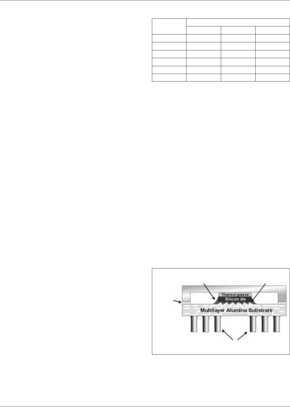
14.1.3 Ceramic Column Grid Arrays (CGA) Solder col-
umn contacts typical of that illustrated in Figure 14-3 are
used for larger ceramic-based packages (32.0 mm to 45.0
mm). The package resembles the earlier pin-grid-array but
with closer contact pitch and more fragile leads (columns).
The column contact diameter is approximately 0.5 mm
with its length varying from 1.25 mm to 2.0 mm. The col-
umns are attached to the package either by eutectic
(Sn63Pb37) solder or they are cast in place using 90% Pb
and 10% Sn.
The longer columns typically increase solder joint reliabil-
ity by absorbing a great deal of the stresses created by the
CTE mismatch between the ceramic package and the
board. Longer columns, on the other-hand, may reduce
Table 14-1 JEDEC Standard JEP95
Allowable Ball Diameter Variations for FBGA (mm)
Ball Pitch
Ball Diameter
Minimum Nominal Maximum
0.80 0.45 0.50 0.55
0.80 0.35 0.40 0.45
0.80 0.25 0.30 0.35
0.65 0.35 0.40 0.45
0.65 0.25 0.30 0.35
0.50 0.25 0.30 0.35
IPC-7351-14-03
Figure 14-3 Ceramic Column Grid Array (CGA) Package
(Cross-Sectional View)
Solder Columns
(Sn10Pb90)
Underfil
Solder Balls
(Sn5Pb95)
Sealing
Adhesive
IPC-7351 February 2005
58
标准分享网 www.bzfxw.com 免费下载
electrical performance and will increase the overall pack-
age profile. Also the columns are not as rugged as ball
contact and are susceptible to handling damage.
14.2 General Configuration Issues
14.2.1 Device Outlines
The Grid Array package outlines
detailed in this document are furnished in JEDEC Publica-
tion JEP95. The overall outline specification for the array
device allows a great deal of flexibility as far as lead pitch,
contact matrix pattern and construction. The JEDEC stan-
dards allow for die attachment on either side of the inter-
face structure (cavity up or cavity down). Refer to IPC-
7096 for further definition and interconnect schemes for
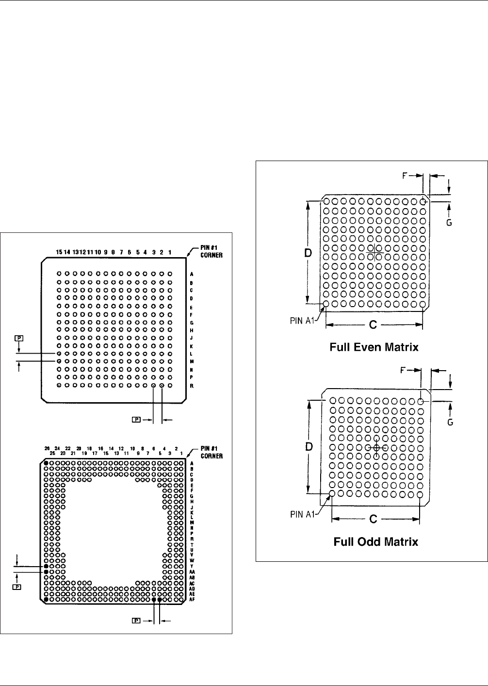
BGAs. The example shown in Figure 14-4 illustrates two
225 I/O devices with a common package outline but, with
the variation of contact pitch, a unique matrix format is
provided.
14.2.2 Contact Matrix Options Contacts may be distrib-
uted in a uniform pattern, however the matrix is always
centered about the centerline of the package (see Figure
14-5). Contact depopulation is permitted at the discretion
of the device manufacturer. Contact patterns can usually be
described in the following methods: full even matrix, full
odd matrix, perimeter matrix, or staggered matrix.
14.2.2.1 Full Matrix For a given package size, there are
two full matrix possibilities: even and odd. One of them is
the largest matrix that theoretically could fit on the pack-
age, given the size and pitch of the contacts. The other
matrix is smaller by one row and column (see Figure 14-5).
14.2.2.2 Perimeter Matrix A perimeter matrix is
achieved by removing an array of contacts from the center
of the matrix. Center-depopulation does not affect the cen-
terline of the matrix (see Figure 14-6). In addition, Perim-
eter matrices are usually described by the number of con-
tact perimeters.
IPC-7351-14-04
Figure 14-4 Bottom View of BGA Devices
IPC-7351-14-05
Figure 14-5 One Package Size, Two Full Matrices
February 2005 IPC-7351
59
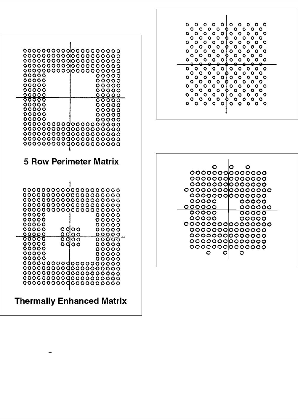
14.2.2.3 Thermally Enhanced Matrix A thermally
enhanced matrix is a perimeter matrix with contacts added
back in the center (see Figure 14-6).
14.2.2.4 Staggered Matrix A staggered matrix is defined
by the removal of every other contact in an interstitial pat-
tern. This provides an effective minimum center-to-center
contact spacing of
√
2 x pitch of the full matrix (see Figure
14-7). In order to retain the A1 contact position, the stag-
gered matrix must be developed using a full odd matrix.
14.2.3 Selective Depopulation In addition to depopula-
tion methods which lead to the matrices described above,
contacts may be removed selectively. Selective depopula-
tion can be accomplished in any manner as long as the pat-
tern matrix is not shifted from the center of the package
outline (see Figure 14-8).
14.2.4 Attachment Site Planning The attachment site or
land pattern geometry recommended for BGA devices is
round with the diameter adjusted to meet contact pitch and
size variation. The diameter of the land should be no larger
than the diameter of the land at the package interface and
is typically 20% smaller than the normal diameter specified
for the ball contact for pitches greater than 1.0 mm and
10% smaller for pitches less than 1.0 mm. Refer to the
manufacturer specification before finalizing land pattern
array and geometry.
14.2.4.1 Copper Defined Land Pattern The land pat-
terns described are defined by the etched copper. Solder
mask clearance should be a minimum of 0.075 mm
[0.00295 in] from the etched copper land. For applications
requiring a clearance that is less than recommended, con-
sult with the printed board supplier.
IPC-7351-14-06
Figure 14-6 Perimeter and Thermally Enhanced Matrices
IPC-7351-14-07
Figure 14-7 Staggered Matrix
IPC-7351-14-08
Figure 14-8 Selective Depopulation
IPC-7351 February 2005
60
标准分享网 www.bzfxw.com 免费下载