IPC-7351-2005_表面贴装焊盘布局设计和标准通用要求.pdf - 第33页
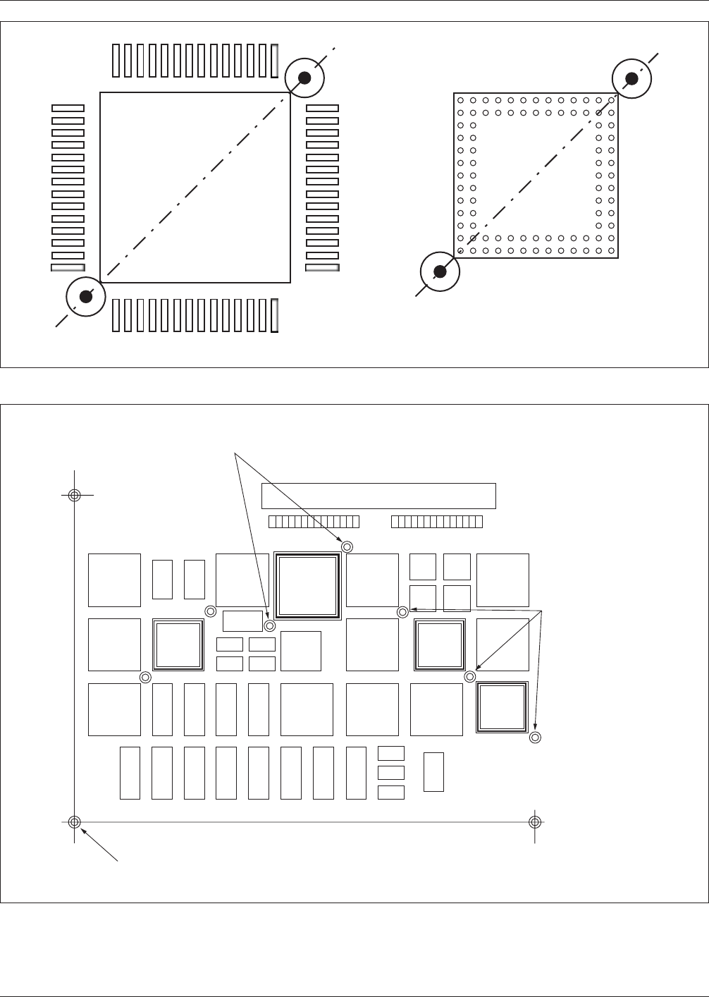
www.bzfxw.com IPC-7351-3-09 Figure 3-9 Local Fiducials T wo Corner Fiducial T argets per FP De vice is Preferred IPC-7351-3-10 Figure 3-10 Fiducial Locations on a Printed Board Global fiducial targets Local fiducial targ…

www.bzfxw.com
making calculations, it should be noted that the solder con-
tent of most pastes is 50% to 55% by volume (not by
weight), depending on particle size.
If the amount of solder paste to be deposited is less than
the amount provided by using an aperture at or near the
land area size, a reduced area of print should be placed in
the best position on the land to assure good wetting of the
joint areas. In some cases, this may best be achieved by
reducing the width of the print, in others, the length. For
very fine pitch with inter-land gaps of less than 0.2 mm,
staggering (offsetting) the print at alternate ends of the
lands can reduce the risk of shorts after soldering.
If the amount of solder paste required is more than the
amount available using the geometry provided for the basic
land pattern on the PCB the aperture size in the stencil can
be enlarged to increase solder volume. The amount and
direction of the overhang of the printed solder beyond the
land is dictated by the space available around the land and
the need to avoid shorting and solder bridging if excess
overhang occurs. The tolerances on land position and print-
ing accuracy need to be considered when calculating the
maximum allowable over-print. See IPC-7525 for the
design and fabrication of stencils for surface mount solder
paste application.
3.4.3 Component Stand-off Height for Cleaning The
recommended minimum component stand-off height for
cleaning is affected by the distance across the diagonal of
the component lead pitch.
If a minimum stand-off cannot be achieved, proper clean-
ing under the component may not be possible. In this case,
it is recommended that a no-clean flux be used and/or mask
material should be retained over all exposed via and circuit
patterns located under devices.
3.4.4 Fiducial Marks A fiducial mark is a printed art-
work feature created in the same process as the circuit art-
work for optical recognition systems. The fiducial and a
circuit pattern artwork must be etched in the same step.
The fiducial marks provide common datum points for all
steps in the assembly process. This allows each piece of
equipment used for assembly to accurately locate the cir-
cuit pattern. There are two types of fiducial marks.
3.4.4.1 Panel and Global Fiducials Global fiducial
marks are used to locate the position of all circuit features
on an individual board. When a multi-image circuit is pro-
cessed in panel form, the global fiducials are referred to as
panel fiducials (see Figure 3-8).
A minimum of two global fiducial marks is required for
correction of offsets (x and y position) and rotational off-
sets (theta position). These should be located diagonally
opposite and as far apart as possible on the circuit or panel.
A minimum of three fiducial marks is required for correc-
tion of nonlinear distortions (scaling, stretch and twist).
These should be located in a triangular position as far apart
as possible on the circuit or panel.
3.4.4.2 Local Fiducials Local fiducial marks are used to
locate the position of an individual component requiring
more precise placement.
A minimum of two local fiducial marks are required for
correction of translational offsets (x and y position) and
rotational offsets (theta position). This can be two marks
located diagonally opposed within or outside the perimeter
of the land pattern (see Figure 3-9).
It is good design practice to locate global or panel fiducials
in a three-point grid-based datum system as shown in Fig-
ure 3-10. The first fiducial is located at the 0-0 location.
The second and third fiducials are located in the X and Y
directions from 0-0 in the positive quadrant. The global
fiducials should be located on the top and bottom layers of
all printed boards that contain surface mount as well as
through-hole components since even through-hole assem-
bly systems are beginning to utilize vision alignment sys-
tems.
All fine pitch components should have two local fiducial
systems designed into the component land pattern to insure
that enough fiducials are available every time the compo-
nent is placed, removed and/or replaced on the board. All
fiducials should have a soldermask opening large enough to
keep the optical target absolutely free of soldermask. If
soldermask should get onto the optical target, some vision
alignment systems may be compromised due to insufficient
contrast at the target site.
If space is limited, one may be able to share a fiducial from
an adjacent component within the location constraint (see
Figure 3-10).
3.4.4.3 Size and Shape of Fiducial The optimum fidu-
cial mark is a solid filled circle. The preferred diameter of
IPC-7351-3-08
Figure 3-8 Panel/Local Fiducials
Panel Fiducial
▼
Global Fiducial
▼
IPC-7351 February 2005
22
标准分享网 www.bzfxw.com 免费下载
www.bzfxw.com
IPC-7351-3-09
Figure 3-9 Local Fiducials
Two Corner Fiducial Targets
per FP Device is Preferred
IPC-7351-3-10
Figure 3-10 Fiducial Locations on a Printed Board
Global fiducial targets
Local fiducial targets for Fine Pitch ICs
F2
F1 F3
Sharing of fiducials
among adjacent
components
February 2005 IPC-7351
23

www.bzfxw.com
the fiducial mark is 1.0 mm. The maximum diameter of the
mark is 3.0 mm. Fiducial marks should not vary in size on
the same PCB more than 25 µm. A clear area devoid of any
other circuit features or markings shall exist around the
fiducial mark. The minimum size of the clear area shall be
equal to twice the radius of the mark (see Figure 3-11).
3.4.4.4 Zonal Fiducials To ensure the accurate place-
ment of multiple surface mount components that are not
near ‘component specific local fiducials’ or ‘global fidu-
cials’, additional ‘zonal fiducial targets’ may be placed
within a zone or an area of the board assembly to compen-
sate for board dimensional stability.
3.4.4.5 Material The fiducial mark may be bare copper,
bare copper protected by organic coating or metal plating.
If solder mask is used, it should not cover the fiducial mark
or the clearance area. It should be noted that excessive oxi-
dation of a fiducial mark’s surface may degrade its read-
ability.
3.4.4.6 Flatness The flatness of the surface of the fidu-
cial mark should be within 15 µm.
3.4.4.7 Edge Clearance The edge of the fiducial should
be no closer to the board edge than the sum of 4.75 mm
and the minimum fiducial clearance required. If less than
this sum, a board handling fixture may be required.
3.4.4.8 Contrast Best performance is achieved when a
consistent high contrast is present between the fiducial
mark and the PCB base material.
The background for all fiducial marks must be the same.
That is, if solid copper planes are retained under fiducials
in the layer below the surface layer, all fiducials must retain
uniform background. If copper is clear under one fiducial,
all must be clear.
3.4.5 Conductors
3.4.5.1 Conductor Width and Spacing
Increased com-
ponent density on SMT designs has mandated the use of
thinner copper, narrower conductor width and spacing.
Higher component density may increase PCB layer counts
as well, requiring the use of more vias to make the neces-
sary connections between layers (see Figure 3-12).
3.4.5.2 Inner Layer Conductors The use of wider con-
ductors and spacing often drives layer counts up because
there is less routing channel available between vias. It is
for this reason that there is an increased usage of narrower
conductors on internal layers. Figure 3-13 compares the
number of routing channels available between lands using
the 0.15 mm geometry. Since conductor width control is
much more difficult to maintain on outer layers of the PCB,
it is better to keep the narrower conductor geometries on
the inner layers of a multilayer printed board. Generally,
the option of using narrow geometries is driven by the need
to reduce layer counts. Decreasing layer counts may reduce
the overall board thickness and improve the aspect ratio for
small hole drilling.
3.4.6 Via Guidelines
3.4.6.1 Drilled Via Holes
The size of the via holes
should be selected on the basis of the printed board thick-
ness versus the hole diameter or aspect ratio limits as
defined by the printed board fabricator. In addition, specific
via lands and holes can be accessed for automatic in-circuit
test (ICT). Figure 3-14 shows the land-pattern-to-via rela-
tionships.
3.4.6.2 Vias and Land Pattern Separation For reflow
soldering, via lands must be located away from the compo-
nent lands to prevent solder migration. This migration will
cause insufficient solder fillets on components. The solder
migration can be restricted by providing a narrow conduc-
tor between the land area and the via or prevented by using
the soldermask over bare copper circuitry. The relationship
for mounting land and via locations should consider the
conductor routing requirements. Figure 3-15 provides sev-
eral examples of via positioning concepts.
Wide conductors connecting to a land area can act as a sol-
der thief by drawing solder away from the land and down
the conductor. Furthermore, if the conductor goes to a via
which is connected to an inner layer power or ground
plane, the plane may act as a heat sink and draw heat away
from the land/lead area during reflow solder resulting in a
defective solder joint.
Specifying soldermask tented or filled vias will prevent
solder migration on assemblies manufactured with a solder
reflow process. Filled or tented vias also take care of poten-
tial flux entrapment problems under components and are
highly desirable for attaining good vacuum seal during
in-circuit bed-of-nails testing. Tenting is typically done
with a dry film type of soldermask, or if via holes are very
small, may be plugged and tented using liquid soldermask.
IPC-7351-3-11
Figure 3-11 Fiducial Size and Clearance Requirements
R
2R
Clearance
Minimum
▼
▼
▼▼
IPC-7351 February 2005
24
标准分享网 www.bzfxw.com 免费下载