IPC-7351-2005_表面贴装焊盘布局设计和标准通用要求.pdf - 第80页
Land P attern Pin A1 on Upper Left Pin A1 on Upper Left Land P attern Ball Grid Array Components P acka ge Outline Component Examples Zero Rotation BGA BGA Rectangular Figure 16-1 Zero Component Rotations for Common Pack…
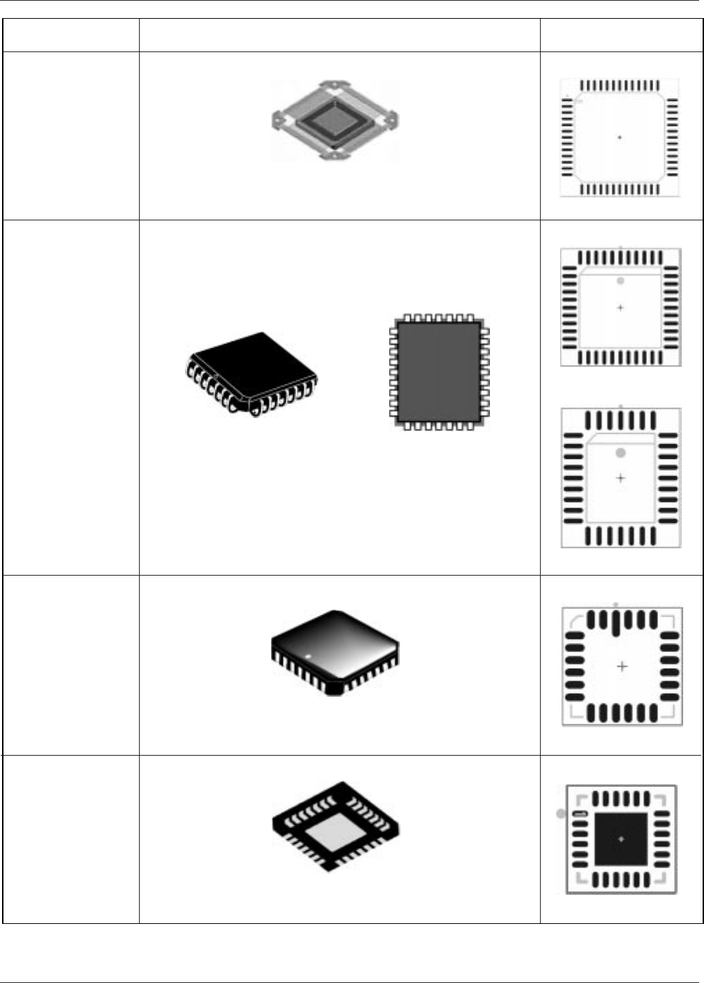
Pin 1 on Top Center
Leadless Chip
Carriers
Quad Flat
No-Lead
Components
Land Pattern
Pin 1 on Upper Left
Land Pattern
Package Outline Component Examples
Zero Rotation
Ceramic Quad
Flat Packages
Pin 1 on Upper Left
Land Pattern
Land Pattern
Land Pattern
Plastic Leaded
Chip Carriers
CQFP
Pin 1 on Top Center
Pin 1 on Top Center
PLCC Square
PLCC Rectangular
Figure 16-1 Zero Component Rotations for Common Package Outlines (continued)
February 2005 IPC-7351
69
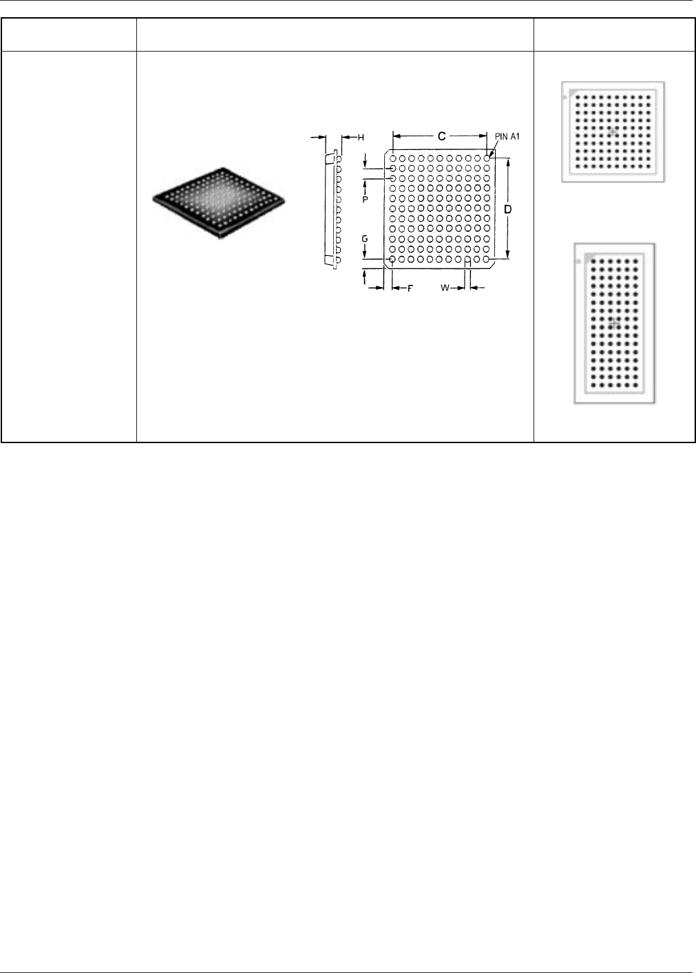
Land Pattern
Pin A1 on Upper Left
Pin A1 on Upper Left
Land Pattern
Ball Grid Array
Components
Package Outline Component Examples
Zero Rotation
BGA
BGA Rectangular
Figure 16-1 Zero Component Rotations for Common Package Outlines
IPC-7351 February 2005
70
标准分享网 www.bzfxw.com 免费下载
Appendix A
(Informative)
Test Patterns – Process Evaluations
The following test patterns have been developed as stan-
dards that may be used for the evaluation of standard board
materials, with a variety of standard parts. IPC-A-49 art-
work is available for these tests. The land patterns repre-
sent land pattern designs from the original IPC-SM-782
land pattern standard.
The test specimen contains conductors and plated-through
holes and parts connected in a single daisy chain. One end
of the daisy chain is connected to a common ground while
the other end of the chain is connected to land patterns,
then to a plated-through hole in which a wire may be sol-
dered for test purposes.
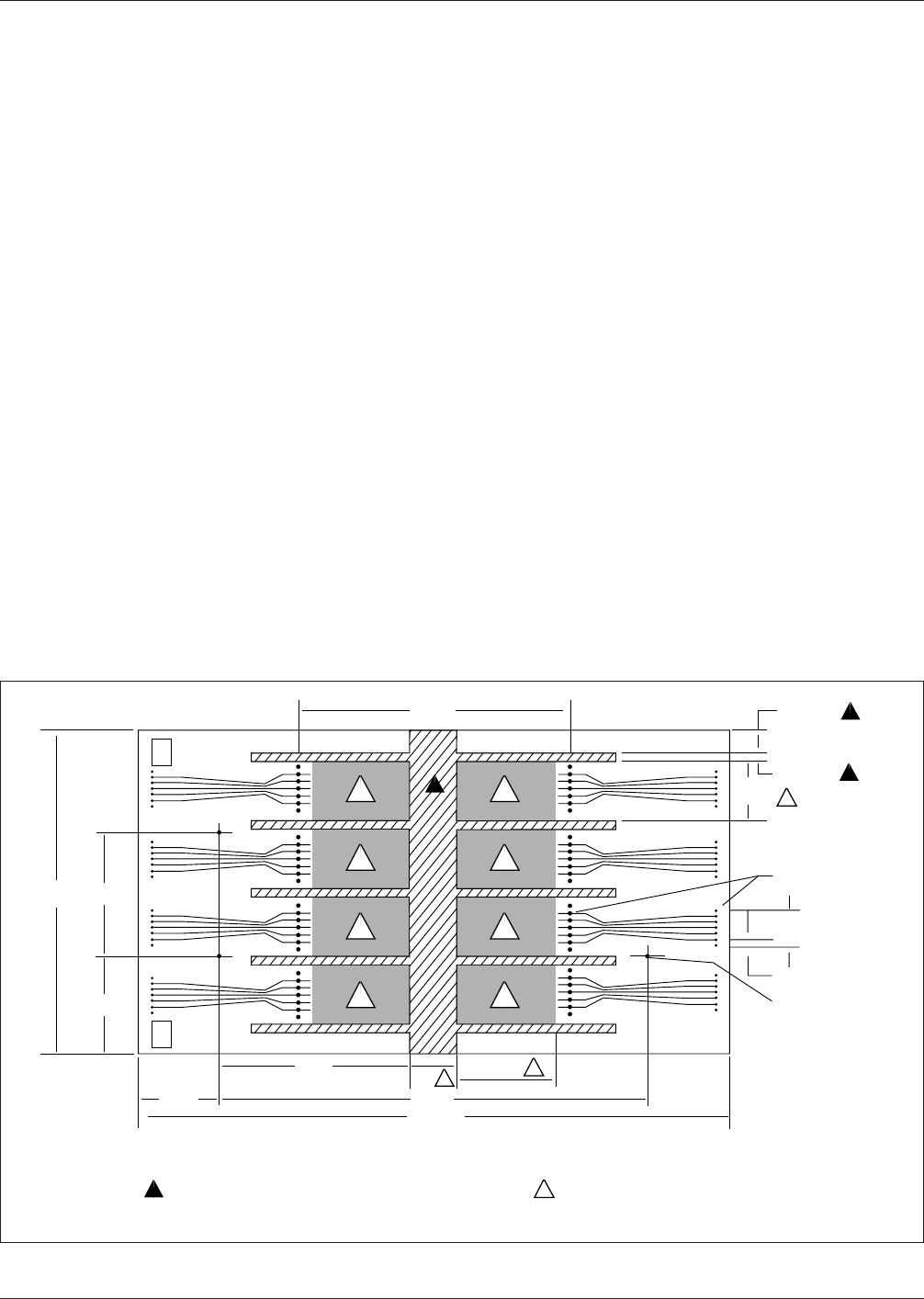
Circuits that are shown in Figure A-1 and Figure A-2 con-
tain the various components listed:
A.1 Test Vehicle Another test specimen is used for the
testing of printed board structures that are intended to pro-
vide P&I structures used primarily for the mounting of
leadless chip carriers. This test board is described in sur-
face mount Air Force Mantech artwork (IPC-A-48). The
board is a 12-layer multilayer board which contains 38
positions for mounting leadless chip carriers used by a sur-
face mount evaluation program to evaluate printed board
and substrate materials. The test boards produced from this
artwork may contain metal cores, or other planes that con-
trol the coefficient of thermal expansion of the P&I struc-
ture.
The following are some examples of the type of materials
that may be used as the constraining core.
a) Nonorganic materials (alumina)
b) Porcelainized clad invar materials
c) Printed boards bonded to low-expansion support (metal
or nonmetal)
d) Compliant layer constructions
e) Metal core boards
A.2 Test Patterns - In-Process Validator Test patterns
to validate in-process conditions are encouraged to be
incorporated into the panel of a printed board assembly.
These designed-in land patterns provide special features for
automatic optical inspection and visual inspection.
IPC-7351-a-01
Figure A-1 General Description of Process Validation Contact Pattern and Interconnect
5
5
5
5
5
5
5
5
+ 41023 -
+ 1 2 -
4 0 3
+ 41023 -
+ 1 2 -
4 0 3
+ 41023 -
+ 1 2 -
4 0 3
+ 41023 -
+ 1 2 -
4 0 3
+ 14032 -
+ 4 3 -
1 0 2
+ 14032 -
+ 4 3 -
1 0 2
+ 14032 -
+ 4 3 -
1 0 2
+ 14032 -
+ 4 3 -
1 0 2
5.600
▼
▼
▼
▼
I.D.I.D.
2.500
▼
▼
2.125
6.745
▼
▼
1.000
4.010
REF
▼
▼
1.490
▼
▼
4
REF
9.020
▼
▼
4
12 ± 1/32
▼
▼
Note: 1. Board G-10 thickness 0.040 - 0.036 2. Primary (top) side
3. Secondary (bottom) side, left-right mirror image
No pattern or components in those
indicated areas allowed 8 sites for test components
5
0.505 REF
▼
▼
▼
▼
▼
▼
▼
▼
▼
▼
▼
0.140 TYP
1.260
TYP REF
4
5
4
0.035 ± 0.003 DIA,
96 HOLES, PTH
0.600 ± 0.003 TYP
0.100 ± 0.003 TYP
0.125 DIA,
3 HOLES
12
3
4
56 7
8
4
2.000 REF
5
▼
▼
▼
▼
▼
All dimensions are in inches
February 2005 IPC-7351
71