IPC-7351-2005_表面贴装焊盘布局设计和标准通用要求.pdf - 第41页
completely cover the conductor . A more precise registration is necessary because of the tight tolerance needed to cover the conductors without encroaching on the land area. PCB manufacturers are required to keep the sol…
www.bzfxw.com
Panel construction may include several boards arranged in
a matrix or simply one board requiring additional material
retained for efficient assembly processing. The large board
or several smaller boards are retained in the panels and
separated after all assembly processes are completed.
Excising or separating the individual boards from the panel
must be planned as well. Several methods are used to retain
circuits in a panel, including V-groove scoring, NC routing
and routed slot with break-away tabs.
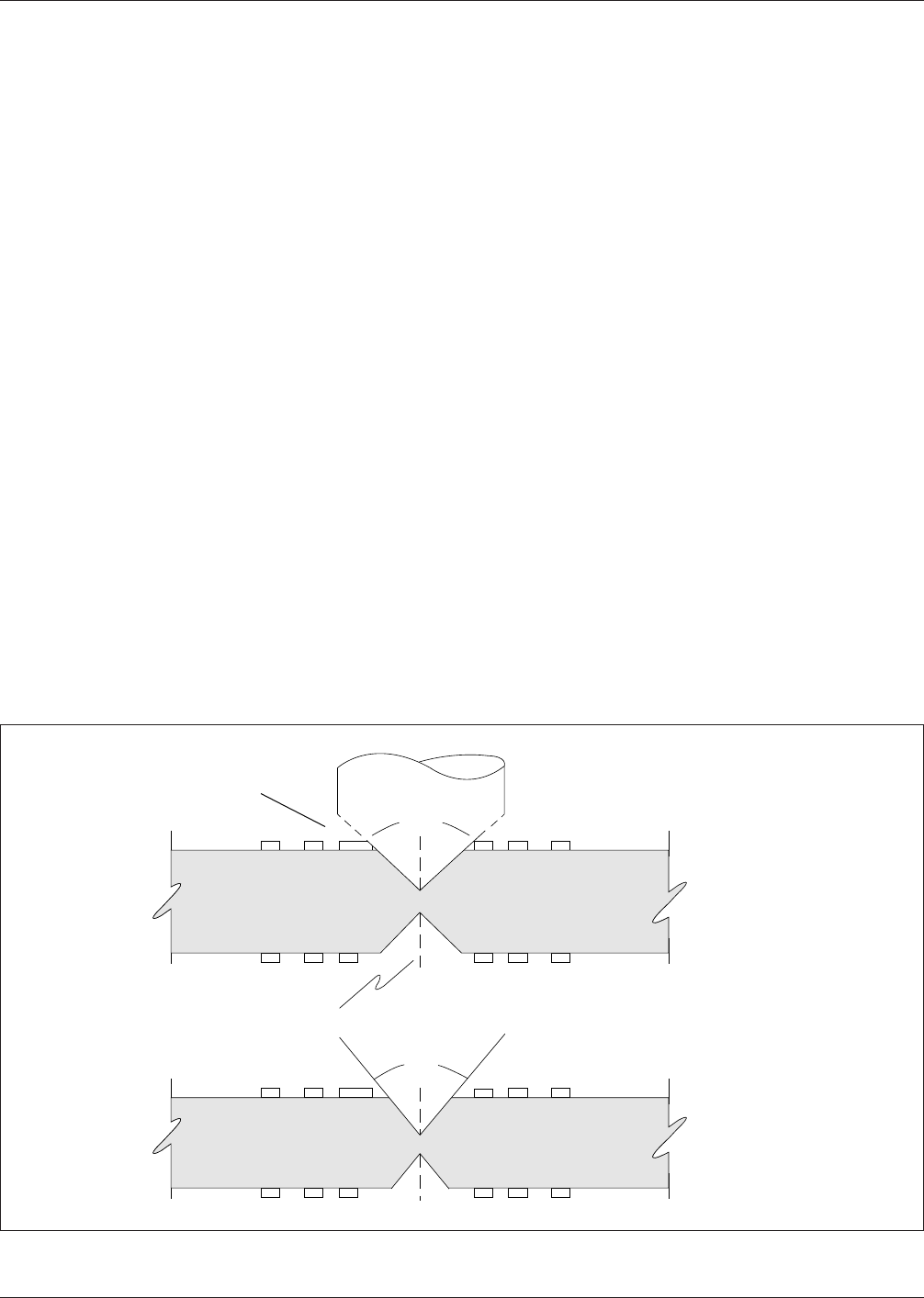
3.4.8.2 V-Groove Scoring V-groove scoring may be pro-
vided to enable post assembly separation. The groove fea-
ture is generally provided on both surfaces of the board and
only in a straight line. A small cross-section of board mate-
rial is retained at the break line. An allowance for the scor-
ing angle must be made as well. Conductors that are
located too close to the score groove will be exposed or
damaged, and rough edges must be sanded lightly to
remove burrs and rough fabric particles (see Figure 3-20).
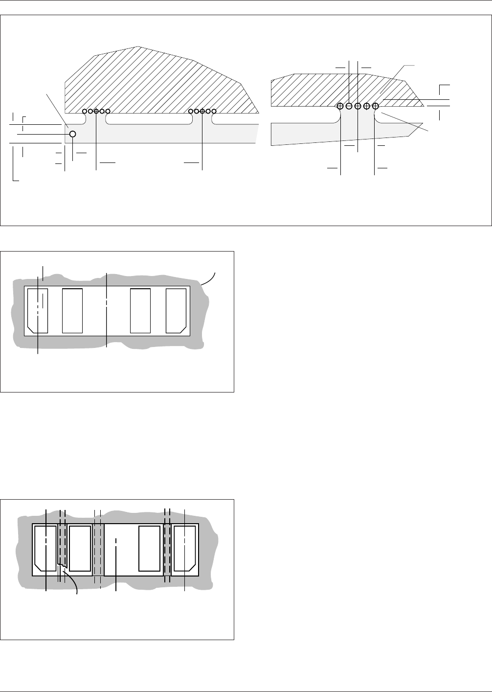
3.4.8.3 Routed Slot and Tab Features The routed slot
and tab pattern is widely used for panel construction and
break-away tab extensions. Routing is more precise than
scoring, and edge surfaces are smooth, but the break-away
‘‘tab’’ points will require consideration. Tabs can be cut
and ground flush with the board edge or predrilled in a pat-
tern. The drilled pattern furnishes a low stress break point
on the ‘‘tab.’’ If the hole pattern is recessed within the
board edge, secondary sanding or grinding can be bypassed
(see Figure 3-21).
3.5 Outer Layer Surface Finishes
3.5.1 Solder Mask Finishes
Solder mask coatings are
used to protect the circuitry on the printed board. Solder
mask coatings are available in two forms, liquid and dry
film. The polymer mask material is applied using several
process methods and is furnished in varying thicknesses.
As an example, liquid materials will have a finished thick-
ness of 0.02 mm [0.0079 in] to 0.025 mm [0.00984 in]
while the dry film products are supplied in thicknesses of
0.04 mm [0.016 in], 0.08 mm [0.0315 in], and 0.10 mm
[0.0394 in]. Although screen type printing for solder mask
is available, photo-imaged soldermask is recommended for
surface mount applications.
The photo process provides a precise pattern image and
when properly developed eliminates mask residue from
land pattern surfaces. The mask thickness may not be a
factor on most surface mount assemblies but, when fine
pitch (0.63 mm [0.0248 in] or less) IC devices are mounted
on the printed boards, the lower profile soldermask will
provide better solder printing control.
3.5.2 Solder Mask Clearances A solder mask may be
used to isolate the land pattern from other conductive fea-
tures on the board such as vias, lands or conductors. Where
no conductors run between lands, a simple gang mask
opening can be used as shown in Figure 3-22.
For land pattern designs with routed conductors between
lands (see Figure 3-23), the solder mask pattern must
IPC-7351-3-20
Figure 3-20 Conductor Clearance for V-Groove Scoring
90˚
▼
▼
Break Line
▼
60˚
▼
▼
Conductors Must
Be Clear of Score
Zone
90˚ Score
Option
60˚ Score
Option
▲
IPC-7351 February 2005
30
标准分享网 www.bzfxw.com 免费下载
completely cover the conductor. A more precise registration
is necessary because of the tight tolerance needed to cover
the conductors without encroaching on the land area. PCB
manufacturers are required to keep the soldermask material
off the land. Clearance conditions can vary from 0.0 mm
[0.0 in] to 0.1 mm [0.0040 in].
3.5.3 Land Pattern Surface Finishes The soldermask
openings expose the land patterns for attachment of surface
mount components. These are usually copper-based and
therefore need protection in order to prevent the copper
from oxidizing, thus resulting in poor solderability of the
surface land patterns. The protection of the land patterns
may be accomplished by organic solderability protective
(OSP) coatings or metallic finishes such as solder coating,
gold, silver, or palladium platings.
The choice of coatings or plating is dependent on the
assembler’s preference or the type of components being
assembled. A single coating or plating finish is preferred
for the entire board. Mixing the surface finish types is not
recommended due to the different process steps required.
Selective finishes may be necessary based on the mix of
component types, lead pitch and attachment process or lead
termination finish characteristics.
4 COMPONENT QUALITY VALIDATION
4.1 Validation Techniques
Because of the variety of
component tolerances, and the possibility that tolerances
may vary on components, users are encouraged to establish
validation of the land pattern and component geometry. In
addition, components should be selected and qualified to
meet the end products maximum operating temperature
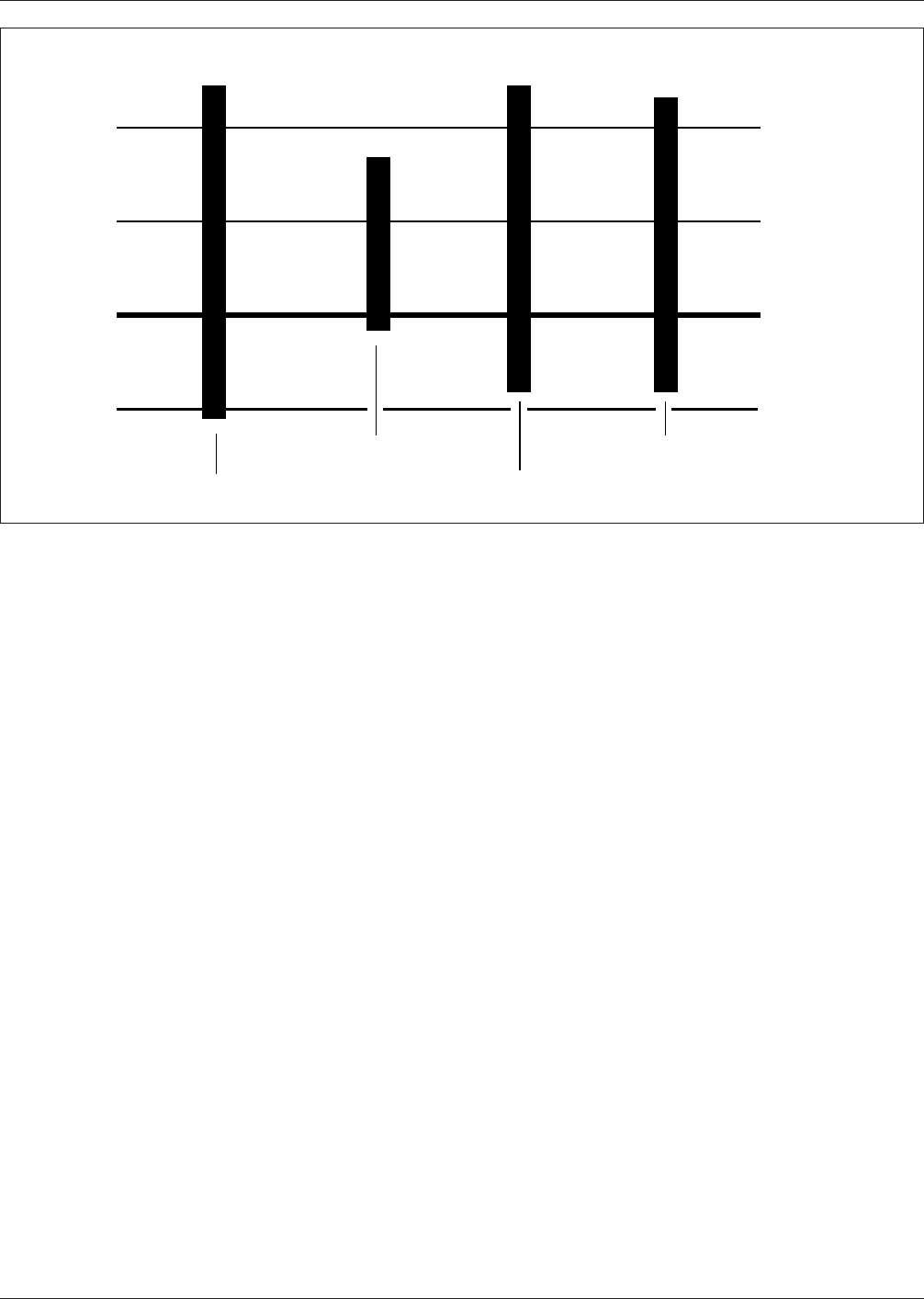
limits. Figure 4-1 shows a chart referencing the upper and
lower limits of various components.
Validations of parts and circuits may be accomplished
through the use of standard test patterns. These patterns
may be used not only to evaluate a particular part to a land
pattern, but may also be used to evaluate component prod-
ucts’ capability to stand up to various processes being used
in assembling surface mounted parts.
IPC-7351-3-21
Figure 3-21 Breakaway (Routed Pattern) with Routed Slots
75 mm [3.0 in] TYP
Approximately
Center to Center Spacing
▼
▼
▼
▼ ▼
▼
▼
▼
▼
0.4 mm
[0.159 in]
Tooling Hole
5.0 mm
[0.197 in]
10 mm [0.40 in]
Depending on PWB
Outline Design
5.0 mm
[0.197 in]
12.5 mm
[0.50 in]
Breakaways
▼
▼
▼
▼
▼
1.25 mm [0.050 in] TYP
0.8 mm [0.031 in]
Dia Thru XX PL
▼
▼
▼
▼
2.25 mm
[0.90 in]
1.2 mm [0.047 in]
R TYP
4.5 mm
[0.180 in]
REF
Detail of Breakaway
▼
▼
0.4 mm
[0.016 in]
LOW STRESS (MOUSE BITE) BREAKAWAY
IPC-7351-3-22
Figure 3-22 Gang Solder Mask Window
Solder Mask
Land
Gang
▼
▼
▼
C
L
IPC-7351-3-23
Figure 3-23 Pocket Solder Mask Window
Land
Conductor
▼
C
L
Pocket
February 2005 IPC-7351
31
5 TESTABILITY
5.1 Board and Assembly Test
There are five basic types
of tests which can be performed on SMT boards. These
are:
a) Bare-board test which checks the unpopulated board for
shorts and opens
b) Manufacturing defect analysis which checks the popu-
lated board for soldering shorts
c) In-circuit test operational verification of each individual
component
d) Functional test operational verification of functional
block of circuits
e) Combinational test limited integration of in-circuit and
functional test
The first test type is a bare-board test performed by the
board fabricator. The remaining four test types are loaded
on assembled board tests and performed after assembly.
The bare-board test should be mandatory, while the loaded
board may be tested using any one or a combination of the
four loaded board tests.
5.1.1 Bare-Board Test In testing printed boards using
through-hole technology, the defect rate and the test meth-
ods chosen are the principle determiners of overall test
cost. Real-estate considerations (specifically the percentage
of nodes that are available for bed-of-nails probing) are not
a concern, since the holes provide 100% nodal access. In
testing surface mount boards, however, real-estate consid-
erations (in addition to defect rates) have an impact on test
costs, since nodal access determines which test methods
are possible and effective.
The use of design concepts with grid-based 100% nodal
access from either side of the board may be the most eco-
nomical approach from the total process perspective. If the
grid-based test land concept is used, the test fixtures for
bare and assembled board tests will not become obsolete
through later board connectivity revisions if the test nodes
are not moved. Also, if the printed board uses buried vias,
the grid-based test land concept with 100% nodal access
may provide access to buried nets from the ends of the
nets; this is a benefit realized during the bare-board test.
5.1.2 Assembled Board Test The method of test must
be determined prior to design layout. If the defect rate is
relatively high, most boards will require diagnosis, and the
economics of automatic in-circuit test (ICT) will demand
that full nodal access be provided within the board layout.
If the defect rate is low, ICT may be omitted and rely on a
functional test. Extremely low defect levels would theoreti-
cally allow 0 % nodal access (no bed-of-nails test at all),
applying only a simple pass/no-pass test through a common
interface connector.
The major considerations in determining nodal access are:
• Defect rate.
• Diagnostic capability.
• Real-estate impact.
• Board area.
• Layer count.
• Cost impact.
IPC-7351-4-01
Figure 4-1 Component Operating Temperature Limits
125
85
125
120
0˚C
–40–40
–10
–55
Ceramic ICs
Plastic ICs
Capacitors
Resistors
▼ ▼
▼
▼
IPC-7351 February 2005
32
标准分享网 www.bzfxw.com 免费下载