IPC-7351-2005_表面贴装焊盘布局设计和标准通用要求.pdf - 第65页
to provide a hermetic seal around the chip. After these steps, the leaded assembly is attached to the printed board. A postleaded ceramic chip carrier typically has leads sol- dered to metallization on the ceramic packag…
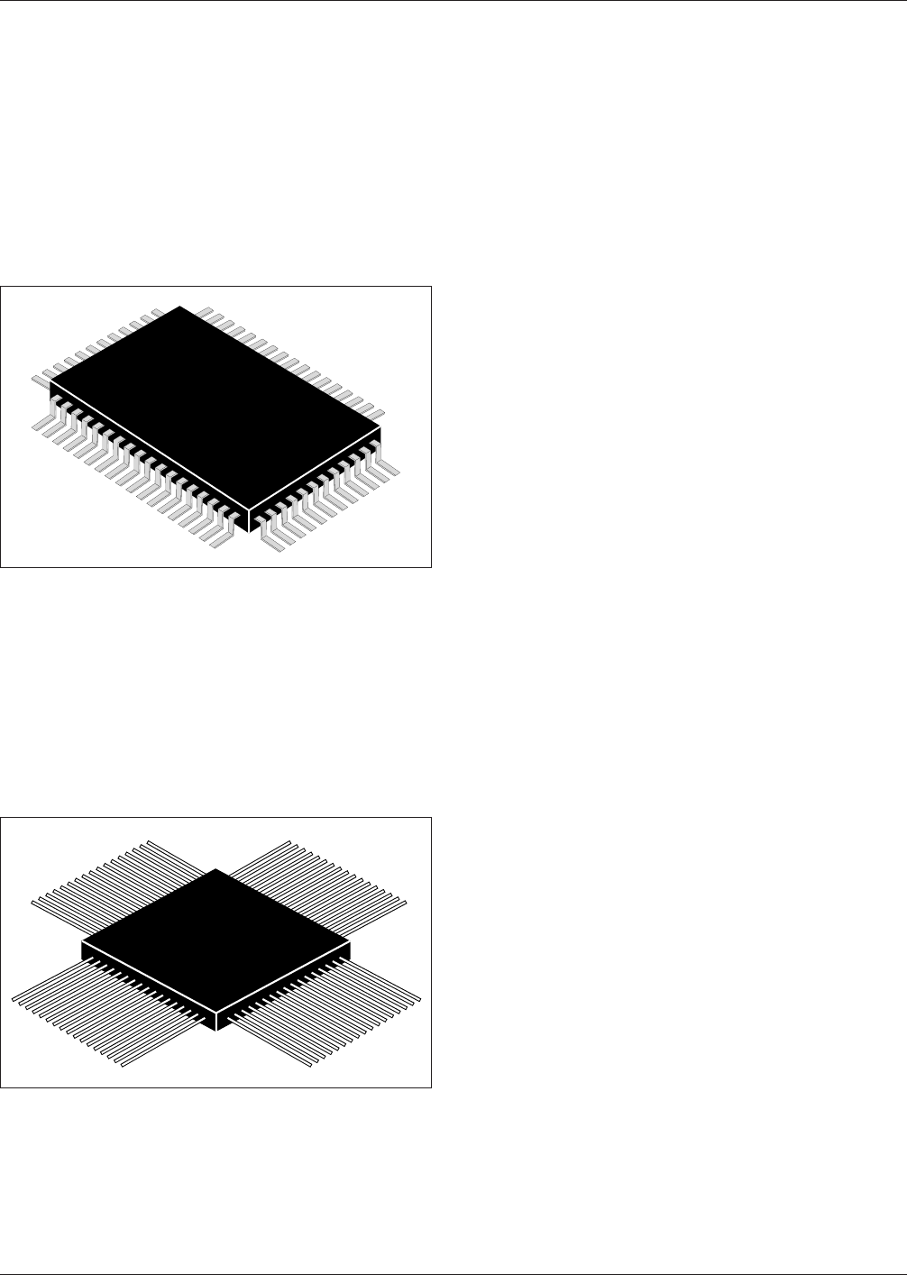
11.3 QFPR The quad flat pack, rectangular (QFPR) has
been developed for applications requiring low height and
high density. The QFPR, along with the TSOP components,
are frequently used in memory card applications. The
QFPR family has leads on a 0.80 mm, 0.60 mm, 0.50 mm,
0.40 mm, or 0.30 mm pitch. IPC-7355 QFPR component
outlines are derived from outline MO-108 within JEDEC
Publication 95 (see Figure 11-3). Two different pin counts
are allowed for each package and the component will still
meet the standard (e.g., a 5x5 package with a 0.3 mm pitch
can have either 56 or 48 pins, and still meet EIAJ-7404-1).
11.3.1 Carrier Package Format The carrier package for-
mat for flat packs may be tube format; but, in most
instances, flat packs are delivered in a carrier tray.
11.4 CQFP See Figure 11-4 for ceramic quad flat pack
(CQFP) construction. Leaded ceramic chip carriers are
typically supplied with an open cavity for chip placement.
Ceramic or metal lids are soldered, epoxied, or attached
with glass frit around the cavity to provide a hermetic seal.
An exception to this construction is the JEDEC standard
outline MS-044, which has the chip bonded to a lead
frame, which is then sealed between two ceramic bodies
with glass frit, similar to CERDIP fabrication. The ceramic
packages are available in 28- through 196-lead configura-
tions, with 1.27 mm, 0.80 mm, and 0.63 mm center spac-
ing. Aside from the MS-044 exception, IPC-7355 CQFP
component outlines are derived from outlines MO-084,
MO-104 and MO-114 within JEDEC Publication 95.
Preleaded ceramic chip carriers typically have copper alloy
or Kovar leads that are attached by the manufacturer. Leads
are typically bonded to metallization on the top surface of
the chip carrier. However, leads can be attached to the
package castellations as well. Brazing or thermo-
compression bonding is usually the attachment means. Pre-
leaded packages using lead-frame construction are also
available. These chip carriers have ceramic bodies with two
opposing halves which mate above and below a lead frame
to which the chip has been previously bonded. The seal is
preformed with glass frit.
Leads can be formed to different shapes, such as ‘‘J,’’ ‘‘L,’’
or ‘‘C’’ configurations. Leads bent in the ‘‘L’’ configuration
are known as ‘‘gullwings.’’
Preleaded chip carriers may be supplied with leads straight
and attached to a common strip. The user must detach the
common strip and form the leads to the desired configura-
tion. This is done to minimize lead bending during ship-
ping and handling. Leads may be supplied pretinned or
with gold plating, as is often done for packages intended
for a high reliability user.
11.4.1 Carrier Package Format Tube carriers are pre-
ferred for best handling.
12 IPC-7356 J LEADED COMPONENTS, FOUR SIDES
Four-sided J-Lead components, also known as Leaded
Chip Carriers, are either ceramic or plastic packages with
terminations which extend beyond the package outlines.
These terminations typically space the body of the package
from the packaging and interconnect structure for reasons
of cleaning, inspecting, or accommodating differences in
thermal expansion. The leads may be attached to the pack-
age body either before or after chip attachment.
In plastic leaded chip carriers, the primary packaging dis-
tinction concerns the point in which a chip is incorporated
into the package. A premolded package is supplied as a
leaded body with an open cavity for chip attachment. A
postmolded body part typically has the chip attached to a
lead frame with an insulating plastic body molded around
the assembly. It is supplied from the manufacturer without
apertures.
Leaded ceramic chip carriers may be similarly classified,
but with a difference in category. The distinction concerns
the point at which leads, if desired, are attached to the
ceramic body. A preleaded ceramic chip carrier is supplied
with copper or Kovar leads brazed to metallization integral
with the ceramic package. Typically, the package is sup-
plied with an open cavity for chip attach. A metal or
ceramic lid is epoxied, soldered, or attached with glass frit
IPC-7351-11-03
Figure 11-3 QFPR Construction
IPC-7351-11-04
Figure 11-4 CQFP Construction
IPC-7351 February 2005
54
标准分享网 www.bzfxw.com 免费下载

to provide a hermetic seal around the chip. After these
steps, the leaded assembly is attached to the printed board.
A postleaded ceramic chip carrier typically has leads sol-
dered to metallization on the ceramic package after chip
attachment. These leads may take the form of edge clips or
solder columns. Incorporation of leads into the assembly
typically occurs immediately prior to board attachment.
High lead-end coplanarity in surface-mounted lead chip
carriers is an important factor in reliable solder attachment
to the printed board. Planarity may be measured from the
lowest three leads of a leaded package. Coplanarity of
0.1 mm [0.004 in] maximum is recommended with 0.05
mm [0.002 in] preferred.
End terminations should be solder coated with a tin/lead
alloy or a lead free equivalent. The solder should contain
between 58 to 68% tin. Solder may be applied to the ter-
mination by hot dipping or by plating from solution. Plated
solder terminations should be subjected to a postplating
reflow operation to fuse the solder. The tin/lead finish
should be at least 0.0075 mm [0.0003 in] thick.
The termination shall be symmetrical, and shall not have
nodules lumps, protrusions, etc., that compromise the sym-
metry or dimensional tolerances of the part. The end termi-
nation shall cover the ends of the components, and shall
extend out to the top and bottom of the component.
Solder finish applied over precious metal electrodes shall
have a diffusion-barrier layer between the electrode metal-
lization and the solder finish. The barrier layer should be
nickel or an equivalent diffusion barrier, and should be at
least 0.00125 mm [0.00005 in] thick.
For lead free finishes a combination of tin, silver and cop-
per is the prevalent replacement for the tin/lead finish. Sol-
derability testing should be applied per IPC-J-STD-002 to
determine attachment capability of the applicable compo-
nent type.
For marking, all parts shall be marked with a part number
and ‘‘Pin 1’’ location. ‘‘Pin 1’’ location may be molded into
the plastic body.
A carrier package format consisting of bulk rods, 24 mm
tape/8-12 mm pitch is preferred for best handling. Tube
carriers are also used.
Parts should be capable of withstanding ten cycles through
a standard reflow system operating at 215 °C [419 °F].
Each cycle shall consist of 60 seconds exposure at 215 °C
[419 °F]. Parts must also be capable of withstanding a
minimum of 10 seconds immersion in molten solder at
260 °C [500 °F]. See IPC/JEDEC J-STD-020 for appropri-
ate reflow cycles and profiles when using lead free solders.
12.1 PLCC Plastic leaded chip carriers (PLCC) are
employed where a hermetic seal is not required. Other con-
straints include limited temperature range (typically 0 °C
[32 °F] or 70 °C [158 °F]) and nominal environmental pro-
tection. As with plastic DIPs, they have the advantage of
low cost as compared to ceramic packages (see Figure
12-1).
12.1.1 Premolded Plastic Chip Carriers The premolded
plastic chip carrier was designed to be connected to the
P&I substrate by means of a socket. Spring pressure on
both sides of the package is intended to constrain move-
ment as well as allow for substrate warpage as high as
0.5%. Solder attach to the P&I substrate is also possible.
The design is also intended to make use of silicone encap-
sulant technology for chip coverage and protection.
12.1.2 Postmolded Plastic Chip Carriers The post-
molded plastic leaded chip carrier is composed of a com-
posite metal/dielectric assembly that includes a conductor
lead frame and a molded insulating body. Compared to the
premolded package which has an aperture for mounting
microelectronic components, the postmolded package
comes complete with no apertures. In both types of plastic
chip carriers, all necessary plating operations are per-
formed by the package manufacturer to eliminate tinning or
plating by the user.
The Joint Device Engineering Council (JEDEC) defines the
Type A Leaded Chip Carrier as a plastic package with leads
wrapped down and around the body on all four sides. This
package can be either directly mounted to a printed wiring
board or used with a socket. It is available with 28, 44, 52,
68, 84, 100, or 124 leads. This family is based on 1.27 mm
lead pitch. The original mechanical outline drawing of this
package was defined based on a premolded package. How-
ever, actual construction is not specified and the package
could be of postmolded construction.
Postmolded packages which have J-lead configurations and
whose outlines are derived from outline MO-047 in JEDEC
Publication are available in 20-, 28-, 44-, 52-, 68-, 84-,
100- and 124-lead counts with the same spacing.
12.2 PLCCR Plastic leaded chip carriers, rectangular
(PLCCR) are employed where a hermetic seal is not
required. Other constraints include limited temperature
IPC-7351-12-01
Figure 12-1 PLCC Construction
February 2005 IPC-7351
55
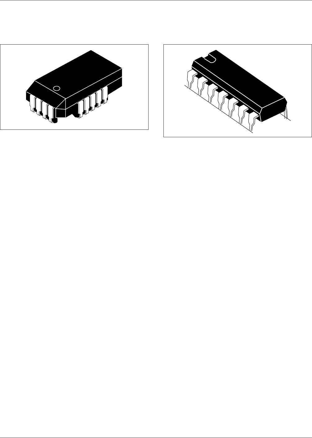
range (typically 0 °C [32 °F] or 70 °C [158 °F]) and nomi-
nal environmental protection. As with plastic DIPs, they
have the advantage of low cost as compared to ceramic
packages (see Figure 12-2).
12.2.1 Premolded Plastic Chip Carriers The premolded
plastic chip carrier was designed to be connected to the
P&I substrate by means of a socket. Spring pressure on
both sides of the package is intended to constrain move-
ment as well as allow for substrate warpage as high as
0.5%. Solder attach to the P&I substrate is also possible.
The design is also intended to make use of silicone encap-
sulant technology for chip coverage and protection.
12.2.2 Postmolded Plastic Chip Carriers The post-
molded plastic leaded chip carrier is composed of a com-
posite metal/dielectric assembly that includes a conductor
lead frame and a molded insulating body. Compared to the
premolded package which has an aperture for mounting
microelectronic components, the postmolded package
comes complete with no apertures. In both types of plastic
chip carriers, all necessary plating operations are per-
formed by the package manufacturer to eliminate tinning or
plating by the user.
The Joint Electron Device Engineering Council (JEDEC)
defines the Type A Leaded Chip Carrier as a plastic pack-
age with leads wrapped down and around the body on all
four sides. This package can be either directly mounted to
a printed wiring board or used with a socket. It is available
with 28, 44, 52, 68, 84, 100, or 124 leads. This family is
based on 1.27 mm lead pitch. The original mechanical out-
line drawing of this package was defined based on a pre-
molded package. However, actual construction is not speci-
fied and the package could be of postmolded construction.
Postmolded packages which have J-lead configurations and
whose outlines are derived from outline MO-047 in JEDEC
Publication are available in 20-, 28-, 44-, 52-, 68-, 84-,
100- and 124-lead counts with the same spacing.
13 IPC-7357 POST (DIP) LEADS, TWO SIDES
A method of modifying DIPs for surface mounting is the
‘‘I’’ mounting technique. This involves simply cutting the
DIP leads to a short length and placing the device on a pat-
tern of lands to be soldered along with the other surface
mounted devices. Construction is usually made of plastic
or ceramics (see Figure 13-1).
13.1 Termination Materials End terminations should be
solder coated with a tin/lead alloy or a lead free equivalent.
The solder should contain between 58 to 68% tin. Solder
may be applied to the termination by hot dipping or by
plating from solution. Plated solder terminations should be
subjected to a postplating reflow operation to fuse the sol-
der. The tin/lead finish should be at least 0.0075 mm
[0.0003 in] thick.
The termination shall be symmetrical, and shall not have
nodules lumps, protrusions, etc., that compromise the sym-
metry or dimensional tolerances of the part. The end termi-
nation shall cover the ends of the components, and shall
extend out to the top and bottom of the component.
Solder finish applied over precious metal electrodes shall
have a diffusion-barrier layer between the electrode metal-
lization and the solder finish. The barrier layer should be
nickel or an equivalent diffusion barrier, and should be at
least 0.00125 mm [0.00005 in] thick.
For lead free finishes a combination of tin, silver and cop-
per is the prevalent replacement for the tin/lead finish. Sol-
derability testing should be applied per IPC-J-STD-002 to
determine attachment capability of the applicable compo-
nent type.
13.2 Marking Parts shall be marked with the part num-
ber and a date code. In addition, pin 1 shall be identified.
13.3 Carrier Package Format Carrier format may be
tubes or as agreed to between user and vendor.
13.4 Resistance to Soldering The parts should be
capable of withstanding ten cycles through a standard
reflow system operating at 215 °C [419 °F]. Each cycle
shall consist of a minimum of 60 seconds exposure at
215T°C [419 °F]. See IPC/JEDEC J-STD-020 for appropri-
ate reflow cycles and profiles when using lead free solders.
IPC-7351-12-02
Figure 12-2 PLCCR Construction
IPC-7351-13-01
Figure 13-1 DIP Construction
IPC-7351 February 2005
56
标准分享网 www.bzfxw.com 免费下载