IPC-7351-2005_表面贴装焊盘布局设计和标准通用要求.pdf - 第51页
need to make a photo tool eliminates the potential for mis- registration. And since there are no photographic steps, a stencil can be made with excellent positional accuracy and remake reproducibility . The tolerance on …
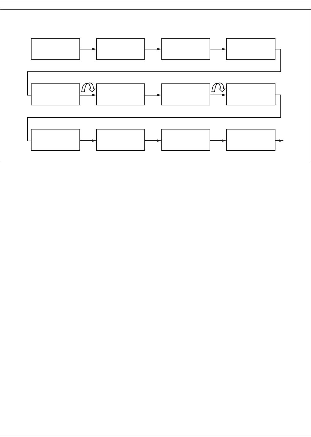
The process sequence for surface mount with through-hole
or pin-in-hole (PIH) component technology is shown in
Figure 7-2. Adhesive is applied and the surface mounted
components placed. The adhesive is then cured, and the
board is inverted to receive the through-hole component
leads automatically or by hand insertion. After lead clinch-
ing (if required), and with the through-hole components on
top and the surface mount components beneath, the board
is typically wave soldered. An alternative sequence is to
reverse the initial stages i.e., insert (and clinch) the
through-hole components before attaching the surface
mounted components and then wave soldering.
Finally the assembly may be cleaned, inspected, repaired if
necessary, and tested, though not necessarily in that order.
7.2 Substrate Preparation
7.2.1 Adhesive Application In wave soldering surface
mount components, selection and application of adhesive
plays a critical role. With too much adhesive, the adhesive
flows onto lands resulting in poor solder fillets. Too little
adhesive will fail to accomplish its objective of holding
parts to the bottom of the board during wave soldering.
7.2.2 Conductive Adhesive Some applications for SMT
attachment use conductive adhesive as the attachment
material. Unlike solder paste which is redistributed when
reflowed, conductive adhesives must be properly controlled
to ensure joint strength. Also, component placement must
be controlled in order to prevent excessive adhesive
squeeze-out, and possible shorts to adjacent lands.
7.2.3 Solder Paste Application Solder paste plays an
important role in reflow soldering. The paste tacks the
component before reflow. It contains flux, solvent, sus-
pending agent, and alloy of the desired composition. Sol-
der paste is applied on the lands before component place-
ment either by screening, stenciling, or syringe. Screens are
made from stainless steel or polyester wire mesh, and sten-
cils are etched stainless steel, brass, and other stable alloys.
Stencils are preferred for high-volume applications. They
are more durable than screens, easier to align, and can be
used to apply a thicker layer of solder paste, and, where
narrow, point apertures are required for example, for fine-
pitch lands. Electroformed stencils may be required for
very small components such as 0201 capacitors and resis-
tors.
The goal of the technology that’s employed to make the
stencil is to ensure that this transfer is as efficient and com-
plete as possible. There are several post processes that
enhance the stencil’s performance, including electropolish-
ing and trapezoidal section apertures that are created with
laser cut technology
7.2.3.1 Laser Cut Stencil Development Laser cut sten-
cils are produced directly from the customer’s original Ger-
ber file or GenCAM or IPC-2581 data. Eliminating the
IPC-7351-7-01
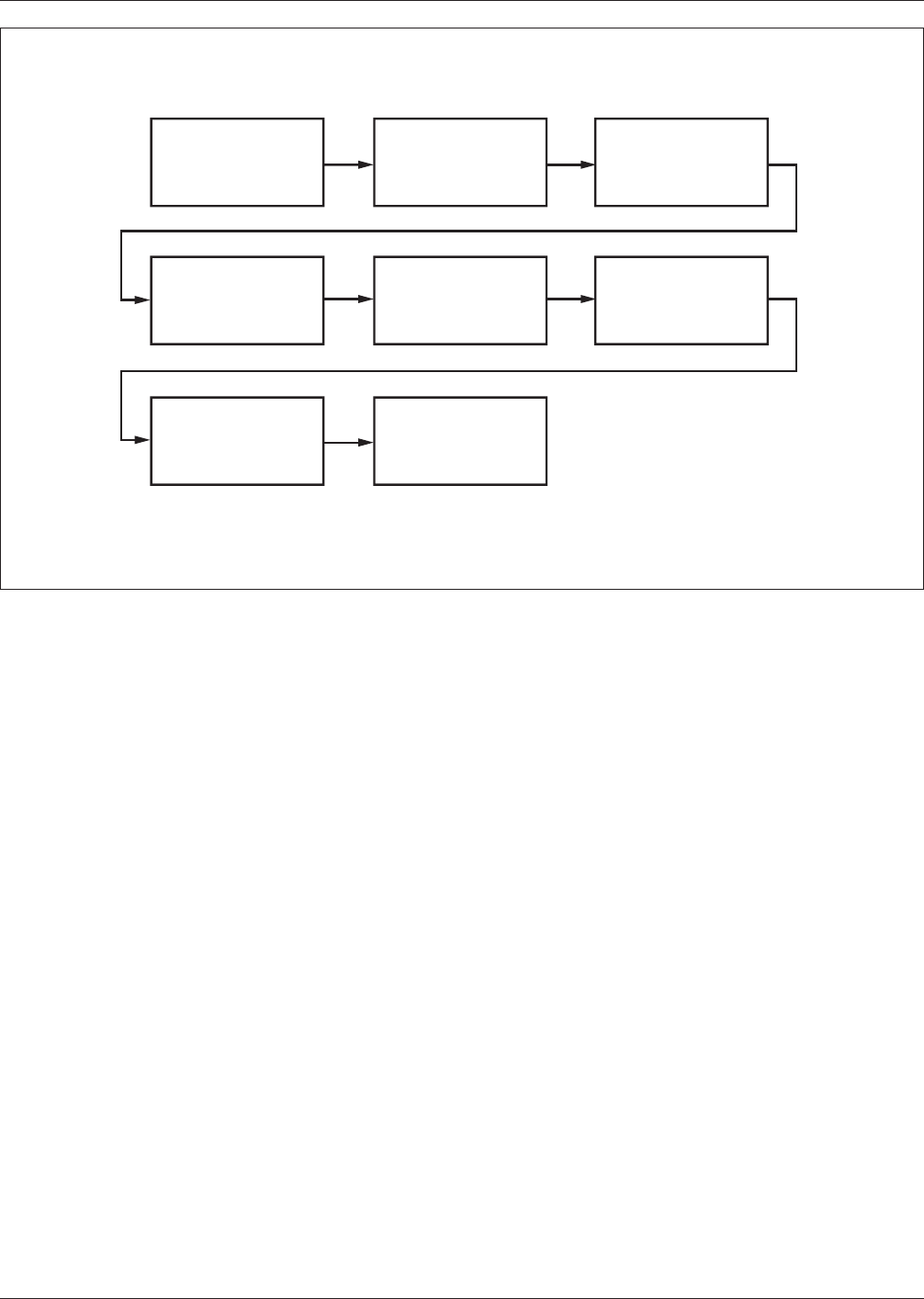
Figure 7-1 Typical Process Flow for Full Surface Mount Type 1b and 2b Surface Mount Technology
Basic Assembly Process for SMT
Solder
Printing
Assembly
Test
2
Package
and Ship
Inspection
Print
Inspection
Reflow
Solder Process
Clean
1
and
Inspection
Device
Placement
1
When cleaning is required.
2
Test may include functional, in-circuit, burn-in as well as post assembly programming.
IPC-7351 February 2005
40
标准分享网 www.bzfxw.com 免费下载
need to make a photo tool eliminates the potential for mis-
registration. And since there are no photographic steps, a
stencil can be made with excellent positional accuracy and
remake reproducibility. The tolerance on the aperture
dimensions can be held to 7 µm [276 µin], allowing for
printing 0.3 mm [0.0118 in] pitch. This process yields
maximum paste release, resulting in minimal stencil clean-
ing, thereby increasing printing efficiency. Plus, the laser
cutting process inherently creates trapezoidal apertures,
furthering complete paste transfer.
A trapezoidal section aperture is one which has a larger
opening on the contact (board) side of the stencil than on
the squeegee side. The opening on the contact side is typi-
cally 5 µm [197 µin] per side larger than the squeegee side
dimension, depending on the customer’s requirements. This
wall geometry, when further enhanced by electropolishing,
allows for better paste release during the printing process.
The results are more noticeable on fine pitch components.
Depending on the overall array design and given the right
metal thickness selection, chem-etched stencils can per-
form adequately at 0.5mm [0.0197 in] pitch. Their effi-
ciency can be improved with performance enhancing pro-
cesses such as electropolishing and/or trapezoidal section
apertures. For more details in the engineering of the stencil
for specific soldering requirements, refer to IPC-7525.
7.2.4 Solder Preforms Solder preforms are sometimes
used for through-hole mounted devices as well as SMT
rework or prototype boards. They come in specific size and
composition, with flux either inside the preforms, or as a
coating or without flux. They may be cost-effective to
avoid wave solder processes if there are only a few leaded
components on the board.
7.3 Component Placement The accuracy requirements
for device placement make it more practical to use roboti-
cally controlled machines for surface mount components
on the board. Selection of the appropriate autoplacement
machine is dictated by the type of components to be placed
and the assembly production rate. Sequential placement
equipment typically utilizes a software controlled X-Y
moving table system. Components are individually placed
on the printed board in succession. Typical cycle times
vary with component size and complexity.
7.3.1 Component Data Transfer Prior to designing the
PCB board in the CAD system, each component is con-
structed in digital form creating an electronic database. The
CAD data is most often used to prepare photo-tool artwork,
PCB fabrication details and assembly instructions but, if
developed in the correct format, it can also be adapted to
manufacturing processes. Direct transfer of CAD data into
automated assembly systems will accelerate production
set-up and reduce overall assembly system programming
time.
When the CAD database for the device is prepared, specific
physical data for each device can be used to assist assem-
bly machine programming for both component placement
(X-Y coordinate position) and orientation. To facilitate the
X-Y coordinate information, a datum position must be
established on the PW board surface. The recommended
datum ‘‘0’’ for X and Y coordinates ideally, may be one of
the global fiducial targets at the lower left or lower right
corner of the board or panel. Surface mount devices are
furnished in tape and reel as well as tube magazine feeders
to accommodate high-speed assembly systems (tray carri-
ers are most often adapted for fine-pitch components).
IPC-7351-7-02
Figure 7-2 Assembly Process Flow for Two-Side Surface Mount with PIH
Two Side SMT / Auto PIH Assembly
Fine Pitch SMT
Placement
Reflow
Solder
Sd. 1 SMT
Placement
Solder Paste
Print
Sd. 2 SMT
Placement
Hand Load
Odd Form PIH
Dispense
Epoxy
Auto Place
PIH
Electrical
Test
Final
Inspection
Clean/
Inspect
Wave
Solder
February 2005 IPC-7351
41

Each surface mount device is aligned using the body cen-
ter and a starting orientation for reference. ‘‘0’’ degree is
the basic orientation of the device.
Rotational data must be specified from the ‘‘0’’ position in
a counter-clockwise direction (typically 90°- 180 - 270).
The ‘‘0’’ starting position of the component is significant.
Tape and reel and JEDEC tray packaged devices for
example, have an established standard for orientation.
The tape-and-reel packaged devices have a predetermined
orientation that is related to the perforated pattern on one
edge of the embossed tape carrier. The standard orientation
does vary, however, between unique device families.
Passive and active devices are supplied in a tape and reel
format, held and protected within an embossed pocket.
Each device family or package type has a standard orienta-
tion in relation to the perforated indexing pattern at the
tape edge.
Orientation as well as polarity of a device must be defined
in the CAD database if the output transferred to assembly
systems is to be reliable. Resistors and capacitor devices
are common in orientation and have no defined polarity. As
the designer develops the component database, numbers
are typically assigned to each end of the device to accom-
modate circuit routing and maintain orientation of value
marking or polarity. Tantalum capacitors, diodes, ICs and
other polarized components, for example, have unique ori-
entation in relation to tape feed systems. Consider the rela-
tionship of the device orientation within the tape cavity to
perforation at the tape carrier material edge.
7.4 Soldering Processes Like the selection of auto-
mated placement machines, the soldering process selection
depends upon the type of components to be soldered and
whether or not they will be used in combination with
leaded parts. For example, if all components are surface
mount types, reflow method (vapor phase, hot air convec-
tion or infrared) may be desirable. However, for through-
hole and surface mount combinations, in mixed technology,
a combination of wave soldering and reflow soldering may
be used. No process is best for all soldering tasks. In addi-
tion, the number of soldering processes discussed in the
following text are by no means complete.
7.4.1 Wave Soldering Wave soldering is an economical
method of soldering mass terminations. There are five to
six main process variables that must be controlled in the
wave soldering process: fluxing, preheat, conveyor speed,
conveyor incline, solder temperature, and possibly cooling
rate.
In preheat, allowance in the conveyer system must be made
for the thermal expansion of the board during preheating
and soldering to prevent board warpage.
In fluxing, flux density, activity and flux foam/flux spray/
flux wave height must be closely monitored. A system must
be in place to determine when the flux activity has deterio-
rated and when the old flux must be replaced and the new
flux added.
Speed is the time sequence and duration of all of the steps
in soldering. By controlling the speed, more uniform and
better joints result. In controlling the conveyer speed, pre-
heating a packaging and interconnecting assembly in two
or three stages minimizes the thermal shock damage to the
assembly and improves its service life. Uniform preheating
is achieved by developing a solder schedule that specifies
preheat settings and conveyer speed for each type of board.
The solder wave is an important variable. Wave geometry
is especially important for preventing icicles and bridges
and for the proper soldering of surface mounted compo-
nents. Wave geometries include uni-directional and
bi-directional; single and double; rough, smooth and dead
zone; oil intermix, dry, and bubbled, and with or without a
hot air knife. Special solder waves just for surface mounted
components are also available.
The concern generally expressed in wave soldering of sur-
face mount devices is damage to the components when
they go through the soldering wave at 260 °C [500 °F]. The
maximum shift in tolerance of resistors and capacitors is
generally found to be 0.2%. This is a negligible amount
considering the part tolerance of commonly used compo-
nents is 5% to 20%. The components generally spend about
three seconds in the wave but they are designed to with-
stand soldering temperatures of 260 °C [500 °F] for up to
ten seconds.
In wave soldering, outgassing and solder skips are two
other main concerns. The outgassing or gas evolution
occurs on the trailing terminations of chip resistors and
capacitors. It is believed to be caused by insufficient drying
of flux and can be corrected by raising the packaging and
interconnecting assembly preheat temperature or time. The
other concern, solder skips, is caused by the shadow effect
of the part body on the trailing terminations. Orienting the
part in such a way that both terminations are soldered
simultaneously solves most shadow effect problems. Some
manufacturers use an extra land to serve as a ‘‘solder
thief’’ for active components.
The most common method for solving both outgassing and
shadow effect is by switching to the dual wave system
where the first wave is turbulent and the second wave is
laminar. The turbulent wave serves to provide an adequate
amount of solder across the surface of the packaging and
interconnecting structure in order to help eliminate outgas-
sing and solder skips. The laminar wave is used to help
eliminate icicles and bridging.
7.4.2 Vapor Phase (VP) Soldering Vapor phase solder-
ing, also known as condensation soldering, uses the latent
heat of vaporization of an inert liquid for soldering. The
IPC-7351 February 2005
42
标准分享网 www.bzfxw.com 免费下载