IPC-7351-2005_表面贴装焊盘布局设计和标准通用要求.pdf - 第46页
in-circuit test. Directions for this should come from test engineering. In addition, it is useful to identify the test vias and lands on an assembly drawing in event of the need to modify the circuit topology . Changes m…
5.7 Printed Board Test Characteristics
5.7.1 Test Land Pattern Spacing
Design for testability
is as much a part of the schematic design process as it is a
part of the board layout process. Ideally, the printed board
would have 100% of the nodes accessable from the second-
ary side of the PB assembly. In-circuit testers must have
access to at least one node per net. Probe spacing is
optional; however, standard probe spacing is typically
2.0 mm [0.0787 in] to 2.5 mm [0.0984 in] while miniature,
needle type probes can be spaced as close as 1.0 mm
[0.0394 in] to 1.25 mm [0.04921 in].
The drawbacks to the 1.0 mm [0.0394 in] to 1.25 mm
[0.04921 in] grid-based test lands are the following. The
miniature, needle type probes are more expensive and they
do not hold up as well in high-volume production. Also,
any via sites that are to be used as test points should be
solder filled for better contact and increased probe life.
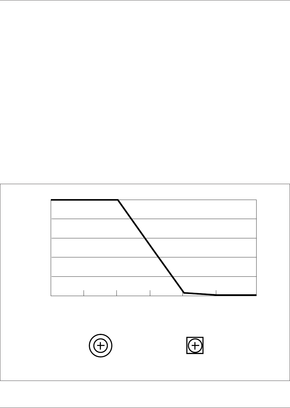
5.7.2 Test Land Size and Shape Lands or vias should be
0.9 mm [0.0354 in] to 1.0 mm [0.0394 in] for probing. As
land sizes decrease, misses increase dramatically as shown
in Figure 5-2. The use of square via lands may provide a
larger target zone for the test probe to contact.
5.7.3 Design for Test Parameters The following other
considerations are important to the general land pattern
design that should be incorporated into the printed board.
a) Two unplated tooling holes should be available on
diagonal corners of the printed board.
b) Test lands should be 2.5 mm [0.0984 in] minimum from
the edge of the printed board to facilitate gasketing on
vacuum fixtures.
c) When using vias for test points, caution should be taken
to insure that signal quality is not degraded at the
expense of testing capability.
d) Test lands should be 0.63 mm [0.0248 in] minimum
from mounting land areas.
e) Where possible, provide numerous test lands for power
and ground.
f) Where possible, provide test lands for all unused gates.
Free running gates sometimes cause instability during
in-circuit testing. This will provide a means of ground-
ing these spurious signals.
It is sometimes desirable to provide drive and sense nodes
test lands to perform six-wire bridge measurements during
IPC-7351-5-02
Figure 5-2 General Relationship Between Test Contact Size and Test Probe Misses
Probability of at Least One Miss
Test/Via Probe Contact Size
100%
80%
60%
40%
20%
0%
0.25 mm 0.35 mm 0.5 mm 0.6 mm
Diameter
0.75 mm
0.9 mm
1.0 mm
1.0 mm Dia
[0.04 in]
0.9 mm Square
[0.036 in]
**
*
*
*
February 2005 IPC-7351
35
in-circuit test. Directions for this should come from test
engineering.
In addition, it is useful to identify the test vias and lands on
an assembly drawing in event of the need to modify the
circuit topology. Changes made without moving test lands
avoid fixture modification, saving cost and time.
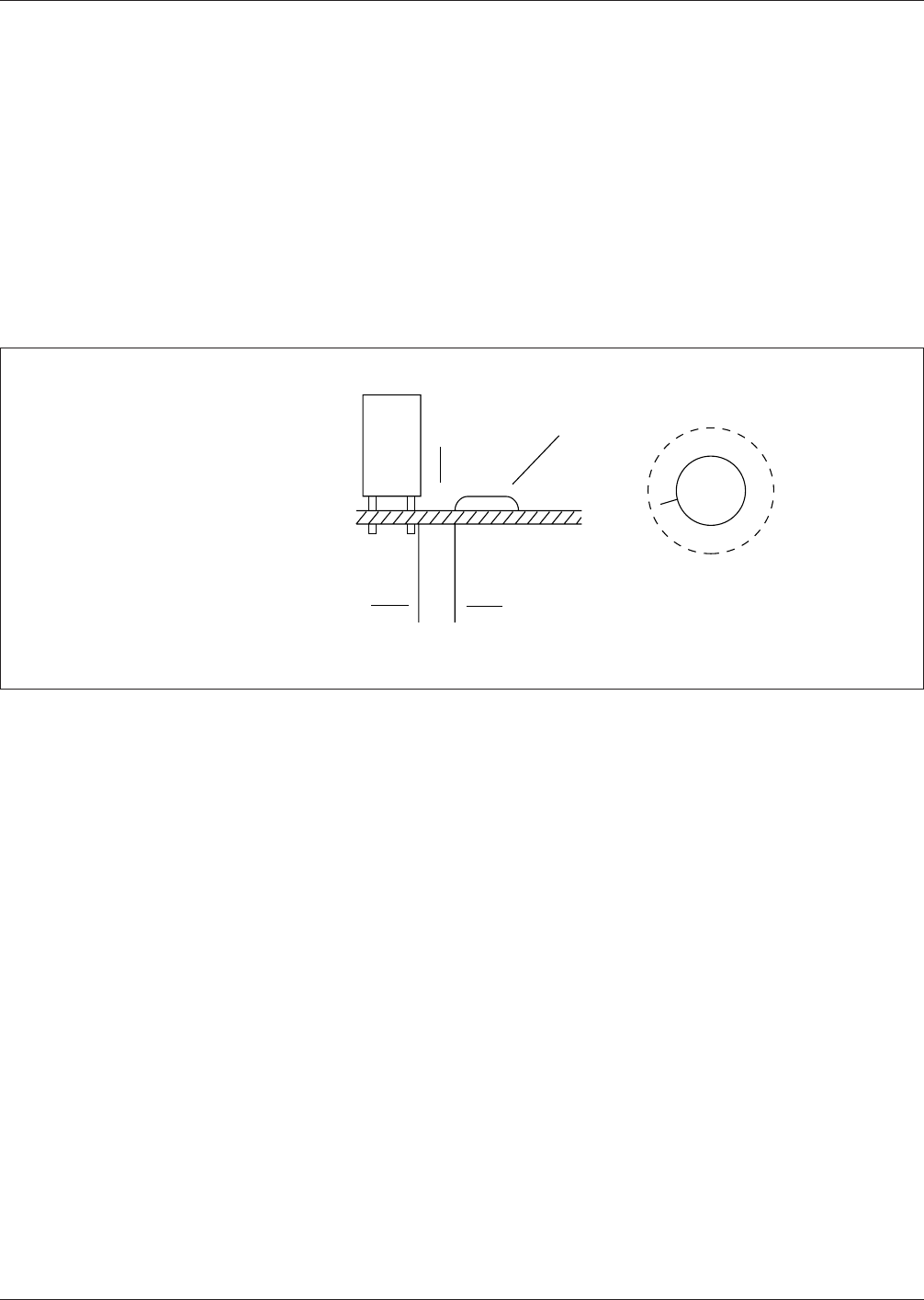
Care should be taken when mounting components on the
secondary side to avoid covering a via hole that is a desig-
nated test land. Also, if a via hole is too close to any com-
ponent, damage may result to the component or fixture
during probing (see Figure 5-3).
6 PRINTED BOARD STRUCTURE TYPES
The selection of a packaging and interconnecting structure
for surface mounting applications is important for optimum
thermal, mechanical and electrical systems reliability. Each
candidate structure has a set of properties with particular
advantages and disadvantages when compared to others
(see Table 6-1).
It is probable that no one packaging and interconnecting
structure or printed board will satisfy all of the needs of the
application. Therefore, a compromise of properties should
be sought that offers the best ‘‘tailoring’’ for component
attachment and circuit reliability.
IPC-7351-5-03
Figure 5-3 Test Probe Feature Distance from Component
Component
Height
▼
▼
▼
Free
Area
6.5 mm [0.256 in] height
> 5.0 mm
[0.20 in] Min.
Test
Pad
5.0 mm [0.20 in]
Tall Component
Free area
▼
▼
Test Pad
IPC-7351 February 2005
36
标准分享网 www.bzfxw.com 免费下载

Table 6-1 Printed Board Structure Comparison
Type Major Advantages Major Disadvantages Comments
Organic Base Substrate
Epoxy fiberglass Substrate size, weight, rework-
able, dielectric properties, con-
ventional board processing.
Thermal conductivity, X, Y and Z
axis CTE.
Because of its high X-Y plane
CTE, it should be limited to
environments and applications
with small changes in tempera-
tures and/or small packages.
Polyimide fiberglass Same as epoxy fiberglass plus
high temperatures X-Y axis
CTE, substrate size, weight,
reworkable, dielectric properties,
high T
g
.
Thermal conductivity, Z-axis
CTE, moisture absorption.
Same as epoxy fiberglass.
Epoxy aramid fiber Same as epoxy fiberglass,
X-axis CTE, substrate size,
lightest weight, reworkable,
dielectric properties.
Thermal conductivity, Z-axis
CTE, resin microcracking, Z
axis CTE, water absorption.
Volume fraction of fiber can be
controlled to tailor X-Y CTE.
Resin selection critical to
reducing resin micro-cracks.
Polyimide aramid fiber Same as epoxy aramid fiber,
X-axis CTE, substrate size,
weight, reworkable, dielectric
properties.
Thermal conductivity, Z-axis
CTE, resin microcracking, water
absorption.
Same as epoxy aramid fiber.
Polyimide quartz (fused
silica)
Same as polyimide aramid fiber,
X-Y axis CTE, substrate size,
weight, reworkable, dielectric
properties.
Thermal conductivity, Z-axis
CTE, drilling, availability, cost,
low resin content required.
Volume fraction of fiber can
be controlled to tailor X-Y CTE,
drill wear-out higher than with
fiberglass.
Fiberglass/aramid
composite fiber
Same as polyimide aramid fiber,
no surface microcracks, Z axis
CTE, substrate size, weight,
reworkable, dielectric properties.
Thermal conductivity, X and Y
axis CTE, water absorption,
process solution entrapment.
Resin microcracks are confined
to internal layers and cannot
damage external circuitry.
Fiberglass/PTFE®
laminates
Dielectric constant, high
temperature.
Same as epoxy fiberglass, low-
temperature stability, thermal
conductivity, X and Y axis CTE.
Suitable for high-speed logic
applications. Same as epoxy
fiberglass.
Flexible dielectric Light weight, minimal concern to
CTE, configuration flexibility.
Size, cost, Z-axis expansion. Rigid-flexible boards offer
trade-off compromises.
Thermoplastic 3-D configurations, low high-
volume cost.
High injection-moulding setup
costs.
Relatively new for these
applications.
Nonorganic Base
Alumina (ceramic) CTE, thermal conductivity,
conventional thick film or thin
film processing, integrated
resistors.
Substrate size, rework limita-
tions, weight, cost, brittle,
dielectric constant.
Most widely used for hybrid
circuit technology.
Supporting Plane
Printed board bonded to
plane support (metal or
nonmetal)
Substrate size, reworkability,
dielectric properties, conven-
tional board processing, X-Y
axis CTE, stiffness, shielding,
cooling.
Weight. The thickness/CTE of the metal
core can be varied along with
the board thickness, to tailor the
overall CTE of the composite.
Sequential processed
board with supporting
plane core
Same as board bonded to
supporting plane.
Weight. Same as board bonded to
supporting plane
Discrete wire High-speed interconnections,
good thermal and electrical
features.
Licensed process, requires
special equipment.
Same as board bonded to low-
expansion metal support plane.
Constraining Core
Porcelainized copper-clad
invar
Same as alumina. Reworkability, compatible thick
film materials.
Thick film materials are still
under development.
Printed board bonded
with constraining metal
core
Same as board bonded to low
expansion metal cores, stiff-
ness, thermal conductivity, low
weight.
Cost, microcracking. The thickness of the graphite
and board can be varied to
tailor the overall CTE of the
composite.
Compliant layer sructures Substrate size, dielectric
properties, X-Y axis, CTE.
Z-axis CTE, thermal
conductivity.
Compliant layer absorbs
difference in CTE between
ceramic package and substrate.
February 2005 IPC-7351
37