IPC-7351-2005_表面贴装焊盘布局设计和标准通用要求.pdf - 第72页
result in a worst case analysis, however as with other land patterns in the standard, a statistical average is determined by using the RMS (root, mean, square) value. T able 14-4 shows the total variation in the system f…
14.2.4.2 Solder Mask Defined Land Pattern If solder
mask defined patterns are used, then adjust land pattern
diameter accordingly (see 14.4).
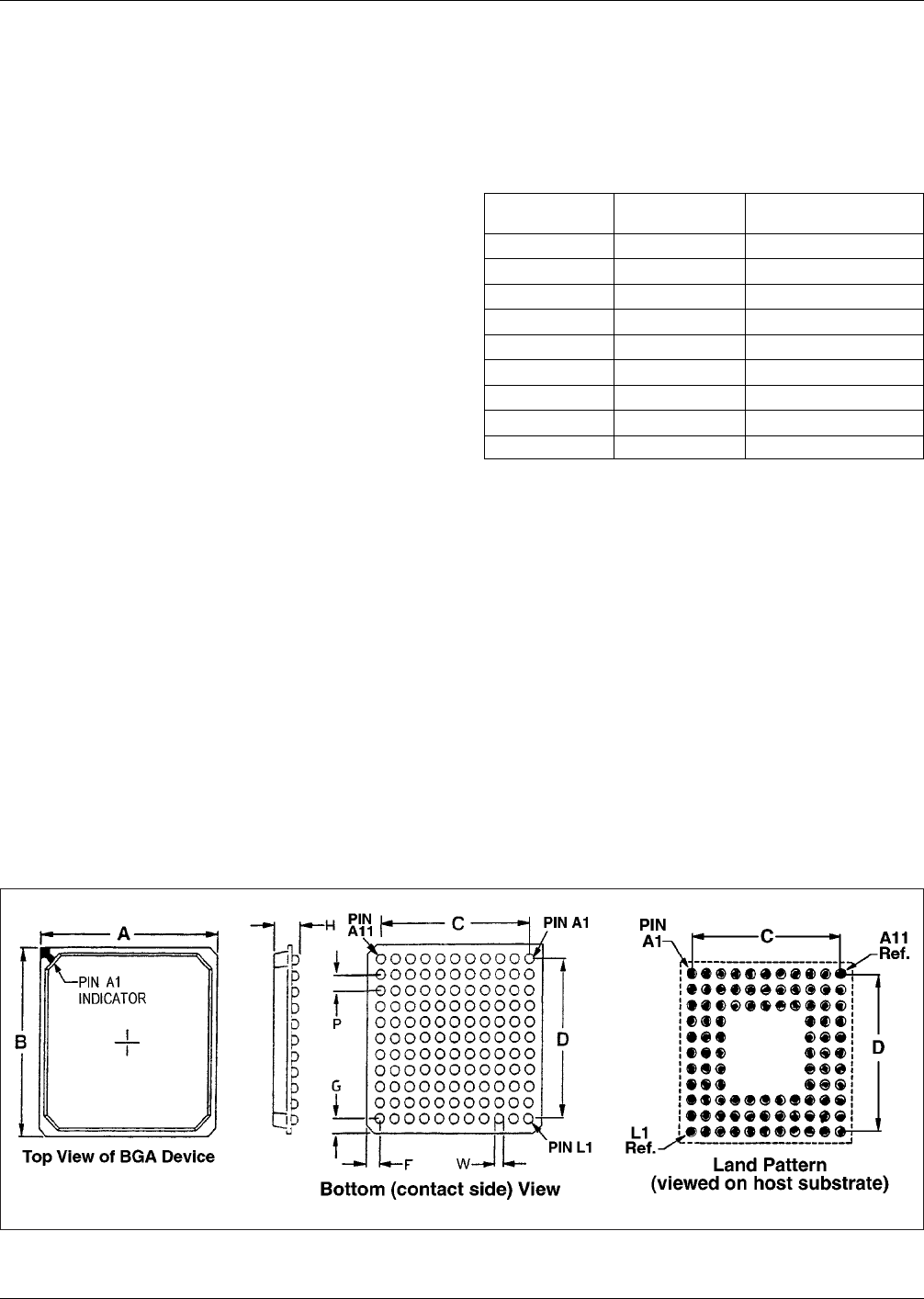
14.2.5 Defining Contact Assignment Array contact
identification is assigned by the column and row location.
For example, A1 contact position is always at an outside
corner position with alpha characters arranged in a vertical
(row) pattern from top to bottom. Numeric characters are
assigned in a horizontal (column) axis (I, O, Q, S, X and Z
are omitted) (see Figure 14-9).
The designer should note that the A1 position is at the
upper left hand corner when the device is viewed from the
top. Contact pattern is defined when viewed from the bot-
tom. The land pattern provided on the host substrate is
opposite of the contact pattern (with A1 contact position
again at the upper left).
14.3 Handling and Shipping For information on trays
and shipping containers refer to ACH:EIA-481-A,
ACH:EIA-481-3, JEDEC CO-028, and JEDEC CO-029.
14.4 Land Pattern Analysis The following provides an
analysis of tolerance assumptions and result in solder joints
based on the land pattern dimensions shown in Figure 14-9.
The variations that exist in determining these land patterns
include the diameter of the individual ball, the positional
accuracy of the ball in relationship to a true position on the
component and the board, and the manufacturing allow-
ance that can be held for the land on the substrate that
mounts the particular ball. The land pattern of the compo-
nent (where the ball is attached) and the land pattern of the
substrate mounting structure (printed board) should be as
similar as possible. Component manufacturers have made
their determinations that the land pattern of pad on the
component should be less than the ball diameter. They base
their conclusions on the resulting nominal ball diameter
with a slight reduction in the land approximation. Pitch
plays a large role in the determination of what ball diam-
eters can be used in various combinations. Table 14-2
shows the characteristics of those balls that are used with
pitches of 1.5 mm through 1.0 mm, as well as future ball
sizes whose pitches fall between 0.40 mm and 0.25 mm.
14.4.1 Land Approximation In each instance, component
manufacturers and board designers are encouraged to
reduce the land size by some percentage of the nominal
ball diameter. The amount of reduction is based on the
original ball size, which is used to determine the average
land. In determining the relationship between nominal
characteristics, a manufacturing allowance for land size has
been determined to be 0.1 mm between the Maximum
Material Condition (MMC) and Least Material Condition
(LMC). Table 14-3 shows the reduction characteristics, the
nominal land size, and the target land dimensions, as well
as future approximations for ball diameters of 0.25 mm and
below.
14.4.2 Total Variation The total variation of the system
considers three major issues: positioning, ball tolerance,
and substrate tolerance. All three attributes added together
IPC-7351-14-09
Figure 14-9 Device Orientation and Contact A1 Position
Table 14-2 Ball Diameter Sizes (mm)
Nominal Ball
Diameter Total Variation Pitch
0.75 0.90 - 0.65 1.5, 1.27
0.60 0.70 - 0.50 1.0
0.50 0.55 - 0.45 1.0, 0.80
0.45 0.50 - 0.40 1.0, 0.80, 0.75
0.40 0.45 - 0.35 0.80, 0.75, 0.65
0.30 0.35 - 0.25 0.80, 0.75, 0.65, 0.50
0.25 0.28 - 0.22 0.40
0.20 0.22 - 0.18 0.30
0.15 0.17 - 0.13 0.25
February 2005 IPC-7351
61
result in a worst case analysis, however as with other land
patterns in the standard, a statistical average is determined
by using the RMS (root, mean, square) value. Table 14-4
shows the total variation in the system for each of the four
ball sizes identified in the standard.
It should be noted that the target value for lands on the
substrate of the component or the board should be at Maxi-
mum Material Condition. The variation from the Maximum
Material Condition indicates that ball-to-land misalignment
is achieved by taking the maximum land size and subtract-
ing the variation. The resulting dimension would indicate
the amount of attachment area that would result from a
system where all conditions are at a negative instance. For
lands that are solder mask-defined, the land size should be
increased by the amount of encroachment of the solder
mask. As an example, if the requirement is that solder
mask should be on the land by 0.05 mm, then the maxi-
mum land size should be increased by 0.1 mm. It should be
noted that for solder mask-defined lands, since the land size
increases, the opportunity to route conductors between
lands is impacted by reducing the available area for con-
ductor width and spacing.
14.4.3 Future Ball Conditions Although not required for
the BGAs shown in the present release of IPC-7351, pro-
jected future ball sizes of 0.40 mm pitch and below are
shown in Table 14-2. Their projected land size approxima-
tions for ball diameters of 0.25 mm and below are shown
in Table 14-3.
14.4.4 Land Pattern Calculator The land pattern calcu-
lations for BGAs are based on ball size. As a result of ball
variation and component conditions, Table 14-5 shows the
land pattern calculator headings needed to describe the
variations in the system. This data is usually described at
the Maximum Material Condition for nonsolder mask-
defined lands and is dimension ‘‘X’’ in the IPC-7351
datasheets for BGA land patterns.
15 IPC-7359 NO LEAD COMPONENTS (QFN, SON, LCC)
15.1 LCC
A leadless chip carrier is a ceramic package
with integral surface-metallized terminations. Leadless
Types A, B, and D chip carriers have a chamfered index
corner that is larger than that of Type C. Another difference
between the A, B, and D types and Type C is the feature in
the other three corners. The types A, B, and D, were
designed for socket applications and printed wiring inter-
connections. The Type C is primarily intended for direct
attachment through reflow soldering. This application dif-
ference is the main reason for their mechanical differences.
These packages mount in different orientations, depending
on type, mounting structure and preferred thermal orienta-
tion.
Table 14-3 Land Approximation (mm)
Nominal Ball
Diameter Reduction
Nominal
Land
Diameter
Land
Variation
0.75 25% 0.55 0.60 - 0.50
0.60 25% 0.45 0.50 - 0.40
0.50 20% 0.40 0.45 - 0.35
0.45 20% 0.35 0.40 - 0.30
0.40 20% 0.30 0.35 - 0.25
0.30 20% 0.25 0.25 - 0.20
0.25 20% 0.20 0.20 - 0.17
0.20 20% 0.15 0.15 - 0.12
0.15 20% 0.10 0.10 - 0.08
Table 14-4 BGA Variation Attributes (mm)
Nominal
Ball Size
Positional
Allowance
Ball
Tolerance
Substrate
Tolerance
Variation
RMS
Value
0.75 0.1 dia. DTP 0.25 0.10 0.25
0.60 0.1 dia. DTP 0.20 0.10 0.24
0.50 0.1 dia. DTP 0.10 0.10 0.17
0.45 0.1 dia. DTP 0.10 0.10 0.17
Table 14-5 Land-to-Ball Calculations for Current and Future BGA Packages (mm)
Land Size
Location
Allowance
Ball
Variation
PCB
Fabrication
Allowance
Ball Size
%
Reduction
from
Nominal
Variation
AllowanceMMC LMC Nominal MMC LMC
0.60 0.50 0.10 0.25 0.10 0.75 0.90 0.65 25% 0.25
0.50 0.40 0.10 0.20 0.10 0.60 0.70 0.50 25% 0.20
0.45 0.35 0.10 0.10 0.10 0.50 0.55 0.45 20% 0.17
0.40 0.30 0.10 0.10 0.10 0.45 0.50 0.40 20% 0.17
0.35 0.25 0.10 0.10 0.10 0.40 0.45 0.35 20% 0.17
0.25 0.20 0.05 0.10 0.05 0.30 0.35 0.25 20% 0.15
0.20 0.17 0.05 0.06 0.03 0.25 0.28 0.22 20% 0.08
0.15 0.12 0.05 0.04 0.03 0.20 0.22 0.18 20% 0.07
0.10 0.08 0.05 0.04 0.02 0.17 0.17 0.13 20% 0.07
IPC-7351 February 2005
62
标准分享网 www.bzfxw.com 免费下载
Leadless Type A is intended for lid-down mounting in a
socket, which places the primary heat-dissipating surface
away from the mounting surface for more effective cooling
in air-cooled systems.
Type C is a ceramic package similar to leadless Type B
except for corner configuration. The 1.27 mm center fam-
ily, which includes both leadless and leaded devices, is
designed to mount on a common mounting pattern. They
may be directly attached to the mounting structure, or can
be plugged into sockets. One basic restriction is that there
shall be no terminals in the corners of the package. There
are a number of common sizes.
End terminations should be solder coated with a tin/lead
alloy or a lead free equivalent. The solder should contain
between 58 to 68% tin. Solder may be applied to the ter-
mination by hot dipping or by plating from solution. Plated
solder terminations should be subjected to a postplating
reflow operation to fuse the solder. The tin/lead finish
should be at least 0.0075 mm [0.0003 in] thick.
The termination shall be symmetrical, and shall not have
nodules lumps, protrusions, etc., that compromise the sym-
metry or dimensional tolerances of the part. The end termi-
nation shall cover the ends of the components, and shall
extend out to the top and bottom of the component.
Solder finish applied over precious metal electrodes shall
have a diffusion-barrier layer between the electrode metal-
lization and the solder finish. The barrier layer should be
nickel or an equivalent diffusion barrier, and should be at
least 0.00125 mm [0.00005 in] thick.
For lead free finishes a combination of tin, silver and cop-
per is the prevalent replacement for the tin/lead finish. Sol-
derability testing should be applied per IPC/EIA-J-STD-
001 to determine attachment capability of the applicable
component type.
15.1.1 Marking All parts shall be marked with a part
number and ‘‘Pin 1’’ location. ‘‘Pin 1’’ location may be
molded into the plastic body.
15.1.2 Carrier Package Format Tube carriers are pre-
ferred for best handling.
15.1.3 Process Considerations LCCs are usually pro-
cessed using standard solder reflow processes. Parts should
be capable of withstanding ten cycles through a standard
reflow system operating at 215° C [419 °F]. Each cycle
shall consist of 60 seconds exposure at 215° C [419 °F].
See IPC/JEDEC J-STD-020 for appropriate reflow cycles
and profiles when using lead free solders.
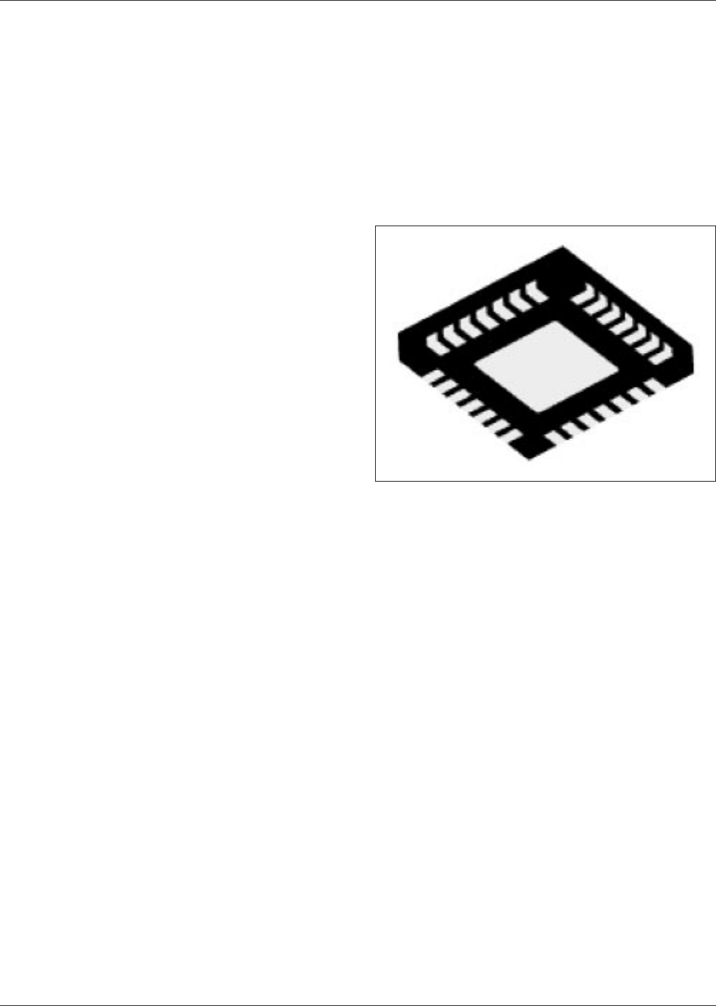
15.2 Quad Flat No-Lead (QFN) The Quad Flat No-Lead
(QFN) package is a near CSP plastic encapsulated package
with a copper leadframe substrate. This is a leadless pack-
age where electrical contact to the PCB is made by solder-
ing the lands on the bottom surface of the package to the
PCB, instead of the conventional formed perimeter leads.
The exposed die attach paddle on the bottom efficiently
conducts heat to the PCB and provides a stable ground
through down bonds or electrical connections through con-
ductive die attach material. The design of the QFN pack-
age also allows for flexibility. Its enhanced electrical per-
formance enables the standard 2 GHz frequency to be
increased up to 10 GHz with some design considerations
(see Figures 15-1 and 15-2).
Solderable areas of the mating surfaces on the end termi-
nations (package bottom side) should be solder coated with
a tin/lead alloy or a lead free equivalent. Ends/sides of the
terminals are not designed as a solderable surface and are
not required to be plated, as this is a physical impossibility
with many current manufacturing processes. Solder may be
applied to the termination by hot dipping or by plating
from solution. Plated solder terminations should be sub-
jected to a postplating reflow operation to fuse the solder.
The tin/lead finish should be at least 0.0075 mm [0.0003
in] thick.
The termination shall be symmetrical, and shall not have
nodules lumps, protrusions, etc., that compromise the sym-
metry or dimensional tolerances of the part. The end termi-
nation shall cover the ends of the components, and shall
extend out to the top and bottom of the component.
Solder finish applied over precious metal electrodes shall
have a diffusion-barrier layer between the electrode metal-
lization and the solder finish. The barrier layer should be
nickel or an equivalent diffusion barrier, and should be at
least 0.00125 mm [0.00005 in] thick.
For lead free finishes a combination of tin, silver and cop-
per is the prevalent replacement for the tin/lead finish. Sol-
derability testing should be applied per IPC-J-STD-002 to
determine attachment capability of the applicable compo-
nent type.
IPC-7351-15-01
Figure 15-1 Quad Flat No-Lead (QFN) Construction
February 2005 IPC-7351
63