IPC-7351-2005_表面贴装焊盘布局设计和标准通用要求.pdf - 第21页
www.bzfxw.com The equations for determining if the clearance ‘ ‘N’ ’ or the attachment overlap ‘ ‘M’ ’ are suf f icient is as follows: M = [ W + X 2 ] − √ C 2 + F 2 + P 2 N = E- [ W + X 2 ] + √ C 2 + F 2 + P 2 3.1.5.1 To…

www.bzfxw.com
3.1.4 Assembly Tolerancing Another part of the equa-
tion is the assembly variation defined by the letter ‘‘P.’’
This variation represents the location of the component in
relation to its true position as defined by the design. The
term diameter of true position (DTP) is used to describe
this variation and is a single number that can be used in the
dimensional tolerance analysis.
As an example, for establishing the target heel protrusion
dimensions of the example shown in Figure 3-3, the fol-
lowing conditions would be true:
Where:
J is 0.5 mm (target heel fillet).
CisS
tol
(RMS) = 1.29 mm (see previous calculations
from component dimensions).
F is 0.1 mm (assumed fabrication tolerance).
P is 0.05 mm (assumed assembly equipment placement
tolerance).
Therefore:
G
min
= 4.55 mm − 2(0.5 mm)−
√
(1.29)
2
+(0.1)
2
+(0.05)
2
= 2.25 mm
Another major condition for multiple-leaded components
that must be considered in land pattern design is lead, ter-
mination, or castellation pitch. The pitch describes the
basic dimension of the spacing of one component lead ter-
mination or castellation to its adjacent counterpart(s). No
tolerance is assigned to pitch in the profile dimensioning
concept. Differences in pitch are included in the width
dimensions of the lead, termination, or castellation which
are dimensioned as basic at the minimum size.
3.1.5 Dimension and Tolerance Analysis In analysing
the design of a component/land pattern system, several
things come into play, including the size and position tol-
erances of the component lead or termination, the toler-
ances of the land pattern, and the placement accuracy of
the man/machine to center the part to the land pattern. The
result is the land area available for a solder joint that pro-
vides a proper formation of a toe, heel, or side fillet.
System equations have been developed for chip compo-
nents and multiple leaded parts. These concepts assume
that the target values of parts and land patterns are maxi-
mized to reflect solder joint formation (i.e., outer dimen-
sions of components at minimum size with outer dimen-
sions of land patterns at maximum size). The equations use
the following symbols:
C is the unilateral profile tolerance(s) for the component.
F is the unilateral profile tolerance(s) for the board land.
pattern
P is the diameter of true position placement accuracy to
the center of the land pattern.
With the assumption that a particular solder joint or solder
volume is desired for every component, some methods use
the worst-case criteria for determining a dimension. This
would require that ‘‘C,’’ ‘‘F,’’ and ‘‘P’’ be added to the
minimum dimension of the component length plus the sol-
der joint requirements, in order to determine the maximum
dimension of the outer land pattern.
Experience shows that the worst-case analysis is not
always necessary; therefore statistical methods are used by
taking the square root of the sum of the squares of the tol-
erances. This method assumes that all features will not
reach their worst case. The equations for determining com-
ponent land pattern requirements are as follows:
Z
max
= L
min
+ 2J
T
+
√
C
L
2
+ F
2
+ P
2
G
min
= S
max
− 2J
H
−
√
C
S
2
+ F
2
+ P
2
X
max
= W
min
+ 2J
S
+
√
C
W
2
+ F
2
+ P
2
Where:
Z is the overall length of land pattern.
G is the distance between lands of the pattern.
X is the width of land pattern.
L is the overall length of component.
S is the distance between component terminations.
Wis the width of the lead or termination.
J is the desired dimension of solder fillet or land
protrusion.
J
T
is the solder fillet or land protrusion at toe.
J
H
is the solder fillet or land protrusion at heel.
J
S
is the solder fillet or land protrusion at side.
C is the component tolerances.
C
L
is the tolerance on component length.
C
S
is the tolerance on distance between component
terminations.
C
W
is the tolerance on the lead width.
F is the printed board fabrication (land pattern geometric)
tolerances.
P is the part placement tolerance (placement equipment
accuracy).
The formula (the square root of the sum of the squares) is
identical for both toe and heel solder joint formation (dif-
ferent tolerances are used, however). However, the desired
solder joint dimension and the square root of the sum of the
squares are added for outer land pattern dimensions and
subtracted for inner land pattern dimensions. The result
provides the final land pattern dimensions Z, G, and X.
The same concept is true for chip, multiple leaded or lead-
less components. Additionally, pitch with lead-to-land
overlap (M) can be evaluated as well as the space (N) to
reflect the clearance between a lead, termination, or castel-
lation and the adjacent land(s). These latter values are not
used in the equations to determine the land pattern sizes,
but may be used to limit lead-to-adjacent land proximity
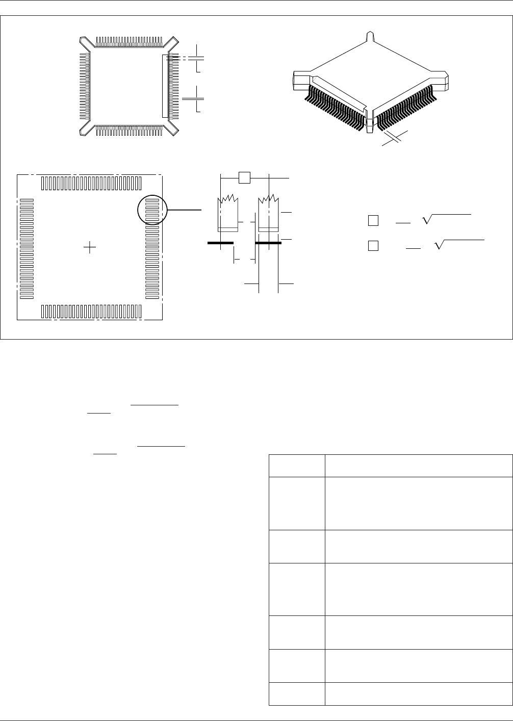
and to adjust lead-to-land overlap (see Figure 3-4).
IPC-7351 February 2005
10
标准分享网 www.bzfxw.com 免费下载
www.bzfxw.com
The equations for determining if the clearance ‘‘N’’ or the
attachment overlap ‘‘M’’ are sufficient is as follows:
M =
[
W + X
2
]
−
√
C
2
+ F
2
+ P
2
N = E-
[
W + X
2
]
+
√
C
2
+ F
2
+ P
2
3.1.5.1 Tolerance and Solder Joint Analysis The fol-
lowing tolerance concepts are used to determine the land
patterns for electronic components. These concepts are
detailed in Table 3-1 and reflect the tolerances on the com-
ponent, the tolerances on the land pattern (on the intercon-
necting substrate), and the accuracy of the equipment used
for placing components.
Solder joint minimums are shown for toe, heel and side fil-
lets. These conditions are minimums, since the equations in
3.1 address the component, board, and placement accuracy
tolerances (sum of the squares). The minimum solder joint
or land protrusion is increased by the amount that the tol-
erance variation does not use up. The courtyard excess is
added to the maximum dimension that the land pattern or
component occupies. The courtyard excess number is
added to each side of the dimension in question. It is
intended that this addition provides sufficient room for
electrical and physical clearance between components
and/or land patterns. Since the total of all the number cal-
culations may not result in a reasonable numerical equiva-
lent, a suggested round-off (up or down) feature has been
added to the tables to identify a rounding up value for the
final number to be used in the design.
IPC-7351-3-04
Figure 3-4 Pitch for Multiple Leaded Components
0.63 Pitch
0.3 - 0.2
▼
▼
Pitch
▼
▼
▼
▼
Leads (W)
Lands (X)
Pitch
▼
▼
E
M
G
M =
W+X
-
C
2
+
F
2
+
P
2
2
Note: Positional tolerance takes angularity into account
N
▼
▼
▼
▼
N = E -
[
W+X
]
-
C
2
+
F
2
+
P
2
2
▼▼
▼
▼
Table 3-1 Tolerance Analysis
Elements for Chip Devices
Tolerance
Element Detailed Description
Component
Tolerance
The difference between the MMC and the
LMC of each component dimension, length,
width and distance between terminations or
leads. This number is the ‘‘C’’ tolerance in
the equations.
Board
Tolerance
The difference between the MMC and the
LMC of each land pattern dimension. This
number is the ‘‘F’’ tolerance in the equations.
Positional
Accuracy
Positional accuracy is defined as diameter
of true position (DTP). This is the variation
of the part centroid related to the land pattern
theoretical center (includes feature location
tolerance from Table 3-17).
Toe Fillet The land protrusion beyond the lead or
termination extremities (see Tables 3-2
through 3-14).
Heel Fillet The land protrusion beyond the internal lead
or termination dimensions (see Tables 3-2
through 3-14).
Side Fillet
Width
The land protrusion to either side of the lead
or termination (see Tables 3-2 through 3-14).
February 2005 IPC-7351
11
www.bzfxw.com
The IPC-7351 Library Documentation spreadsheets
included with this standard provide an analysis of tolerance
assumptions and resultant solder joints based on the fin-
ished land pattern dimensions. Tolerances for component
dimensions, the land pattern dimensions (fabrication toler-
ances on the interconnecting substrate), and the component
placement equipment accuracy are all taken into consider-
ation. These tolerances are addressed in a statistical mode,
and assume even distribution of the tolerances for compo-
nent, fabrication and placement accuracy.
Individual tolerances for fabrication (‘‘F’’) and component
placement equipment accuracy (‘‘P’’) are assumed to be as
given in spreadsheet documentation. These numbers may
be modified based on user equipment capability or fabrica-
tion criteria. Component tolerance ranges (C
L
,C
S
, and C
W
)
are derived by subtracting minimum from maximum
dimensions given. The user may also modify these num-
bers, based on experience with their suppliers.
The dimensions for minimum solder fillets at the toe, heel,
or side (J
T
,J
H
,J
S
) have been determined based on industry
empirical knowledge and reliability testing. Solder joint
strength is greatly determined by solder volume. An
observable solder fillet is necessary for evidence of proper
wetting. Thus, the values in the library documentation
spreadsheets usually provide for a positive solder fillet.
Nevertheless, if the user of any of the three land pattern
geometry variations desires a more robust process condi-
tion for placement and soldering equipment, individual ele-
ments of the analysis may be changed to new and desired
dimensional conditions. This includes component, board or
placement accuracy spread, as well as minimum solder
joint or land protrusion expectation. In addition, this stan-
dard recognizes the need to have different goals for the
solder fillet or land protrusion conditions.
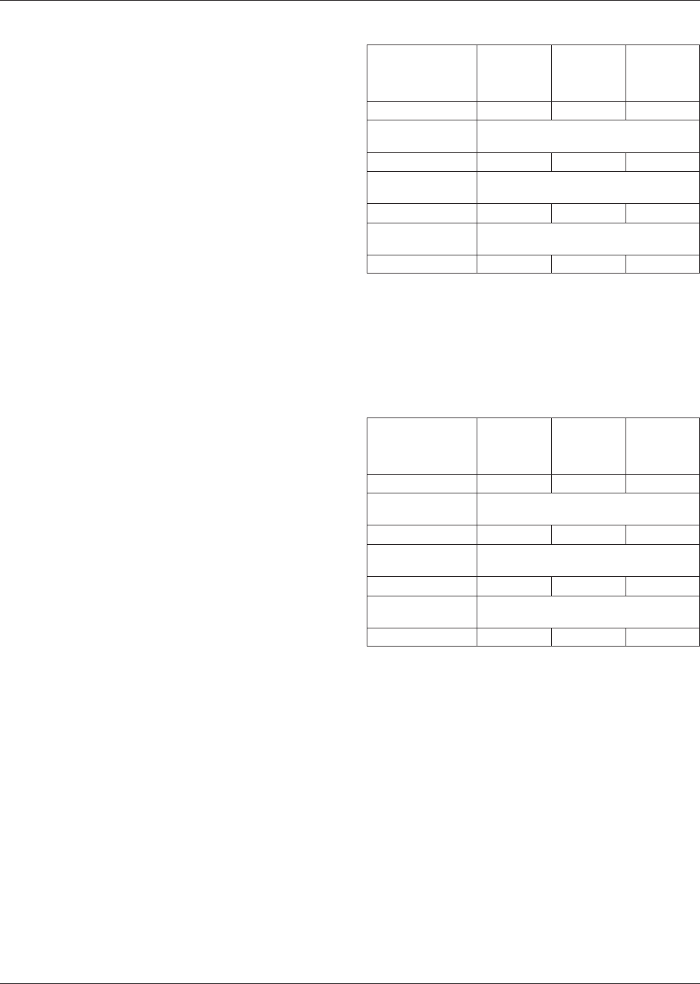
Tables 3-2 through 3-14 indicate the principles used for the
three goals established by this standard. The tables reflect
maximum (most), median (nominal) and minimum (least)
material conditions for the land protrusions used to develop
land patterns for surface mounting various lead or termina-
tions of components. Unless otherwise indicated, the IPC-
7351 identifies all three goals as Density Levels A, B, or C.
3.1.5.2 Component Dimensions Illustrations of compo-
nent dimensions in each library documentation spreadsheet
are accompanied by a table of figures for each of the dif-
ferent part numbers, as taken from multinational compo-
nent standards organizations. The standards organizations
provide many more dimensions to define the requirements
for manufacturing the specific components in a family
class; only those dimensions that are necessary for land
pattern development are repeated within the library docu-
mentation spreadsheets. At times, the component tolerances
or component gauge requirements do not necessarily reflect
the exact tolerance on a manufacturer’s data sheet. Compo-
nent dimensions are provided according to the concepts of
maximum and least materials condition (MMC and LMC).
Both conditions are presented in the tables within the
library documentation spreadsheets. The component manu-
facturers may not always dimension their components in
accordance with the limits shown in the tables. However,
these limits may be used as criteria for go/no-go accep-
tance of the component. The LMC dimensions of the fig-
ure are those that have been used in the equations
described in 3.1 for determining the recommended land
pattern.
Table 3-2 Flat Ribbon L and Gull-Wing
Leads (greater than 0.625 mm pitch) (unit: mm)
Lead Part
Minimum
(Least)
Density
Level C
Median
(Nominal)
Density
Level B
Maximum
(Most)
Density
Level A
Toe (J
T
) 0.15 0.35 0.55
Round-off factor
Round off to the nearest two place
even decimal, i.e., 1.00, 1.20, 1.40
Heel (J
H
)
1
0.25 0.35 0.45
Round-off factor
Round off to the nearest two place
even decimal, i.e., 1.00, 1.20, 1.40
Side (J
S
) 0.01 0.03 0.05
Round-off factor
Round off to the nearest two place
decimal, i.e., 1.00, 1.05, 1.10, 1.15
Courtyard excess 0.1 0.25 0.5
1. For gullwing components where dimension Smin is less than or equal to
dimension Amax, use the following heel fillet goals:
Density Level C - 0.05 mm
Density Level B - 0.15 mm
Density Level A - 0.25 mm
Note: This does not apply to gullwing components where the lead terminals
have a tolerance T1 that is greater than 0.5 mm.
Table 3-3 Flat Ribbon L and Gull-Wing Leads
(less than or equal to 0.625 mm pitch) (unit: mm)
Lead Part
Minimum
(Least)
Density
Level C
Median
(Nominal)
Density
Level B
Maximum
(Most)
Density
Level A
Toe (J
T
) 0.15 0.35 0.55
Round-off factor
Round off to the nearest two place
even decimal, i.e., 1.00, 1.20, 1.40
Heel (J
H
)
1
0.25 0.35 0.45
Round-off factor
Round off to the nearest one place
decimal, i.e., 1.0, 1.1, 1.2, 1.3
Side (J
S
) -0.04 -0.02 0.01
Round-off factor
Round off to the nearest two place
decimal, i.e., 1.00, 1.05, 1.10, 1.15
Courtyard excess 0.1 0.25 0.5
1. For gullwing components where dimension Smin is less than or equal to
dimension Amax, use the following heel fillet goals:
Density Level C - 0.05 mm
Density Level B - 0.15 mm
Density Level A - 0.25 mm
Note: This does not apply to gullwing components where the lead terminals
have a tolerance T1 that is greater than 0.5 mm.
IPC-7351 February 2005
12
标准分享网 www.bzfxw.com 免费下载