IPC-7351-2005_表面贴装焊盘布局设计和标准通用要求.pdf - 第32页
www.bzfxw.com making calculations, it should be noted that the solder con- tent of most pastes is 50% to 55% by volume (not by weight), depending on particle size. If the amount of solder paste to be deposited is less th…
www.bzfxw.com
SMT printed board. With it, the exact location and volume
of solder paste deposition is precisely controlled. The art-
work for developing the stencil is the component mounting
lands from the outer layers of the board with all other cir-
cuitry deleted. The information provided for the openings
in the stencil is usually indicated as being the same size as
the lands on the board for all components. This information
(or data) may be selectively modified by the printed board
assembler or process engineer who will define the specific
adjustments required to meet specific solder volume
requirements (see IPC 7525).
The optimum stencil thickness is determined by evaluating
the solder paste requirements for all the components to be
reflow soldered. This should be based on study of the mini-
mum and target requirements for SMT solder joints given
in IPC/EIA-J-STD-001.
Ideally, the volume deposited should be the total amount
required to achieve the ‘‘target’’ solder joint condition (see
IPC-A-610), less the solder already available on the land
and termination or lead (the latter can together amount to
10% to 20% of the total and should not be ignored). In
IPC-7351-3-06
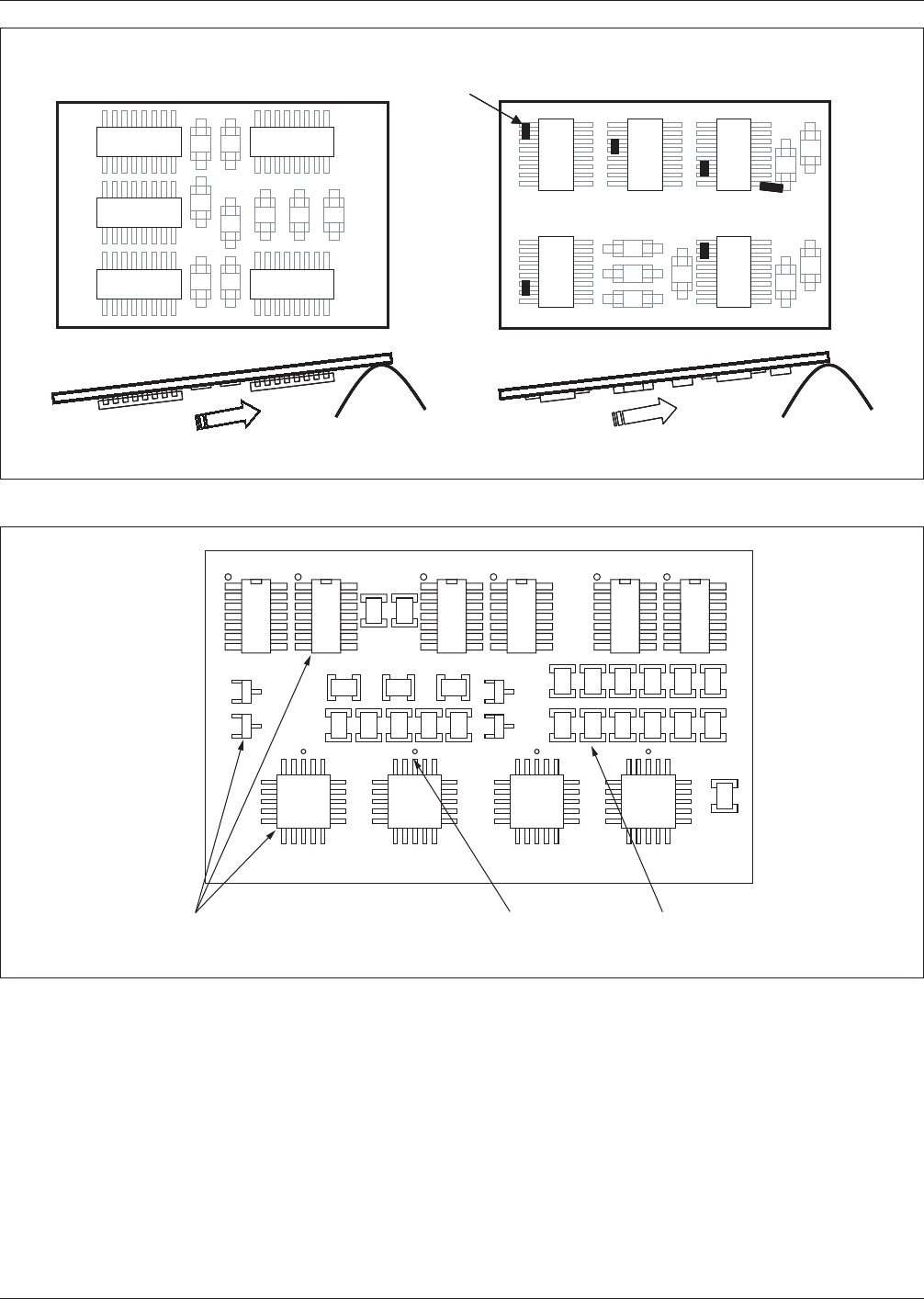
Figure 3-6 Component Orientation for Wave-Solder Applications
Preferred Orientation
Defect Prone Orientation
Solder
bridging
Solder
Wave
Solder
Wave
IPC-7351-3-07
Figure 3-7 Alignment of Similar Components
Consistent
Orientation
Pin 1 I.D. Uniform
Spacing
February 2005 IPC-7351
21

www.bzfxw.com
making calculations, it should be noted that the solder con-
tent of most pastes is 50% to 55% by volume (not by
weight), depending on particle size.
If the amount of solder paste to be deposited is less than
the amount provided by using an aperture at or near the
land area size, a reduced area of print should be placed in
the best position on the land to assure good wetting of the
joint areas. In some cases, this may best be achieved by
reducing the width of the print, in others, the length. For
very fine pitch with inter-land gaps of less than 0.2 mm,
staggering (offsetting) the print at alternate ends of the
lands can reduce the risk of shorts after soldering.
If the amount of solder paste required is more than the
amount available using the geometry provided for the basic
land pattern on the PCB the aperture size in the stencil can
be enlarged to increase solder volume. The amount and
direction of the overhang of the printed solder beyond the
land is dictated by the space available around the land and
the need to avoid shorting and solder bridging if excess
overhang occurs. The tolerances on land position and print-
ing accuracy need to be considered when calculating the
maximum allowable over-print. See IPC-7525 for the
design and fabrication of stencils for surface mount solder
paste application.
3.4.3 Component Stand-off Height for Cleaning The
recommended minimum component stand-off height for
cleaning is affected by the distance across the diagonal of
the component lead pitch.
If a minimum stand-off cannot be achieved, proper clean-
ing under the component may not be possible. In this case,
it is recommended that a no-clean flux be used and/or mask
material should be retained over all exposed via and circuit
patterns located under devices.
3.4.4 Fiducial Marks A fiducial mark is a printed art-
work feature created in the same process as the circuit art-
work for optical recognition systems. The fiducial and a
circuit pattern artwork must be etched in the same step.
The fiducial marks provide common datum points for all
steps in the assembly process. This allows each piece of
equipment used for assembly to accurately locate the cir-
cuit pattern. There are two types of fiducial marks.
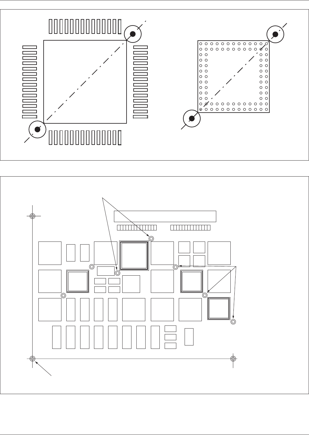
3.4.4.1 Panel and Global Fiducials Global fiducial
marks are used to locate the position of all circuit features
on an individual board. When a multi-image circuit is pro-
cessed in panel form, the global fiducials are referred to as
panel fiducials (see Figure 3-8).
A minimum of two global fiducial marks is required for
correction of offsets (x and y position) and rotational off-
sets (theta position). These should be located diagonally
opposite and as far apart as possible on the circuit or panel.
A minimum of three fiducial marks is required for correc-
tion of nonlinear distortions (scaling, stretch and twist).
These should be located in a triangular position as far apart
as possible on the circuit or panel.
3.4.4.2 Local Fiducials Local fiducial marks are used to
locate the position of an individual component requiring
more precise placement.
A minimum of two local fiducial marks are required for
correction of translational offsets (x and y position) and
rotational offsets (theta position). This can be two marks
located diagonally opposed within or outside the perimeter
of the land pattern (see Figure 3-9).
It is good design practice to locate global or panel fiducials
in a three-point grid-based datum system as shown in Fig-
ure 3-10. The first fiducial is located at the 0-0 location.
The second and third fiducials are located in the X and Y
directions from 0-0 in the positive quadrant. The global
fiducials should be located on the top and bottom layers of
all printed boards that contain surface mount as well as
through-hole components since even through-hole assem-
bly systems are beginning to utilize vision alignment sys-
tems.
All fine pitch components should have two local fiducial
systems designed into the component land pattern to insure
that enough fiducials are available every time the compo-
nent is placed, removed and/or replaced on the board. All
fiducials should have a soldermask opening large enough to
keep the optical target absolutely free of soldermask. If
soldermask should get onto the optical target, some vision
alignment systems may be compromised due to insufficient
contrast at the target site.
If space is limited, one may be able to share a fiducial from
an adjacent component within the location constraint (see
Figure 3-10).
3.4.4.3 Size and Shape of Fiducial The optimum fidu-
cial mark is a solid filled circle. The preferred diameter of
IPC-7351-3-08
Figure 3-8 Panel/Local Fiducials
Panel Fiducial
▼
Global Fiducial
▼
IPC-7351 February 2005
22
标准分享网 www.bzfxw.com 免费下载
www.bzfxw.com
IPC-7351-3-09
Figure 3-9 Local Fiducials
Two Corner Fiducial Targets
per FP Device is Preferred
IPC-7351-3-10
Figure 3-10 Fiducial Locations on a Printed Board
Global fiducial targets
Local fiducial targets for Fine Pitch ICs
F2
F1 F3
Sharing of fiducials
among adjacent
components
February 2005 IPC-7351
23