IPC-7351-2005_表面贴装焊盘布局设计和标准通用要求.pdf - 第17页
www.bzfxw.com formation of the acceptable solder joint. Component manu- facturers usually provide dimensions for their parts with a nominal size and then put a tolerance on that nominal dimension. In order to facilitate …
www.bzfxw.com
2.4 International Electrotechnical Commission
4
IEC-61188 Printed Boards and Printed Board Assemblies -
Design and Use
2.5 Joint Electron Device Engineering Council (JEDEC)
5
Publication 95 JEDEC Registered and Standard Outlines
for Solid State Products
3 DESIGN REQUIREMENTS
3.1 Dimensioning Systems
This section describes a set
of dimensional criteria for components, land patterns, posi-
tional accuracy of the component placement capability and
the opportunity to create a certain size solder joint com-
mensurate with reliability or product performance analysis.
Profile tolerances are used in the dimensioning system to
define the size range between maximum and minimum
component/lead dimensions without ambiguity. The profile
tolerance is intended to control both size and position of
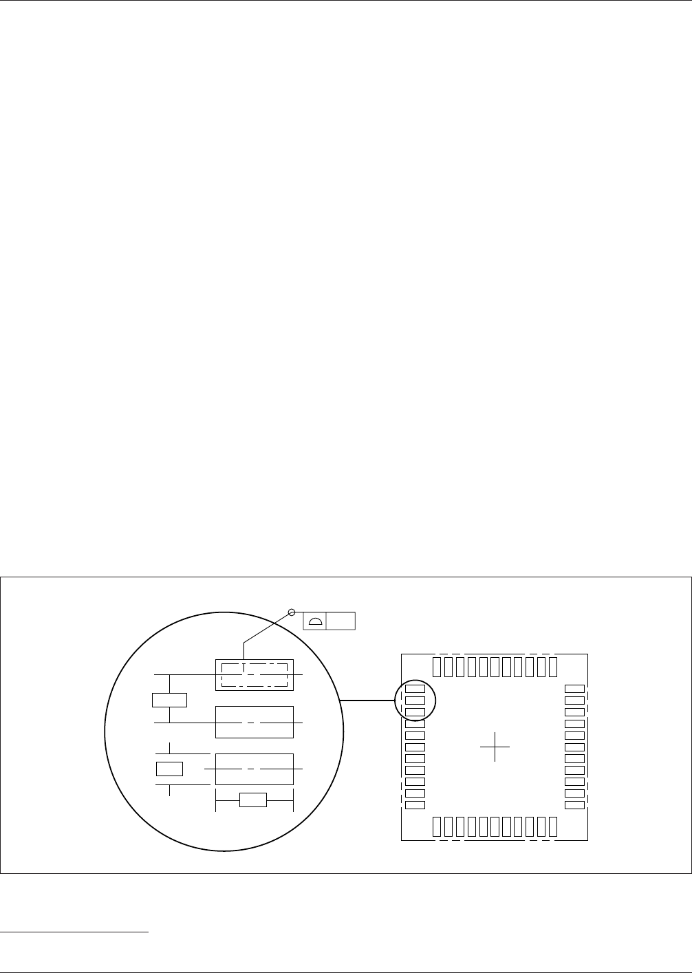
the land. Figure 3-1 shows the profile tolerancing method.
The use of the profile dimensioning system requires an
understanding of the concepts. The use of a set of require-
ments are adopted and invoke the following rules, unless
otherwise modified.
a. All dimensions are basic (nominal).
b. Limits of size control form as well as size.
c. Perfect form is required at maximum dimensions.
d. Datum references and position tolerances apply at maxi-
mum dimensions, and are dependent on feature size.
e. Position dimensions originate from maximum dimen-
sions.
f. Tolerances and their datum references other than size
and position apply regardless of feature size (RFS).
The dimensioning concepts used for this system of analy-
sis consider the assembly/attachment requirements as their
major goal. Specification (data) sheets for components or
dimensions for land patterns on boards may use different
dimensioning concepts, however, the goal is to combine all
concepts into a single system. Users are encouraged to
establish the appropriate relationship between their dimen-
sioning system(s) and the profile dimensioning system and
analysis concepts described herein to allow for ease of tai-
loring these concepts for robust process performance. As
an example, if the tolerance used for positioning is larger
than the machine tolerance used in production, a single
dimensional change could modify the land pattern.
3.1.1 Component Tolerancing The component manu-
facturers and industry standards organizations are respon-
sible for the dimensioning and tolerancing of electronic
components (see 3.1.5.2). The basic dimensions and toler-
ance limits published in the specifications have been con-
verted to a functional equivalent using the profile toleranc-
ing method with all components shown with their basic
dimensions as limit dimensions (maximum or minimum
size). Profile tolerances are unilateral, and are described to
reflect the best condition for solder joint formation.
The concept for component dimension evaluations is based
on evaluating the surfaces of the component termination
and component lead or contact that are involved in the
4. www.iec.ch
5. www.jedec.org
IPC-7351-3-01
Figure 3-1 Profile Tolerancing Method
0.7
1.27
▼
▼
▼
▼
▼
2.5
MMC
▼
▼
▼
0.1
MMC
"
N
"
Places
IPC-7351 February 2005
6
标准分享网 www.bzfxw.com 免费下载
www.bzfxw.com
formation of the acceptable solder joint. Component manu-
facturers usually provide dimensions for their parts with a
nominal size and then put a tolerance on that nominal
dimension. In order to facilitate the dimensioning system,
these dimensions and their associated tolerances are con-
verted to minimum and maximum size.
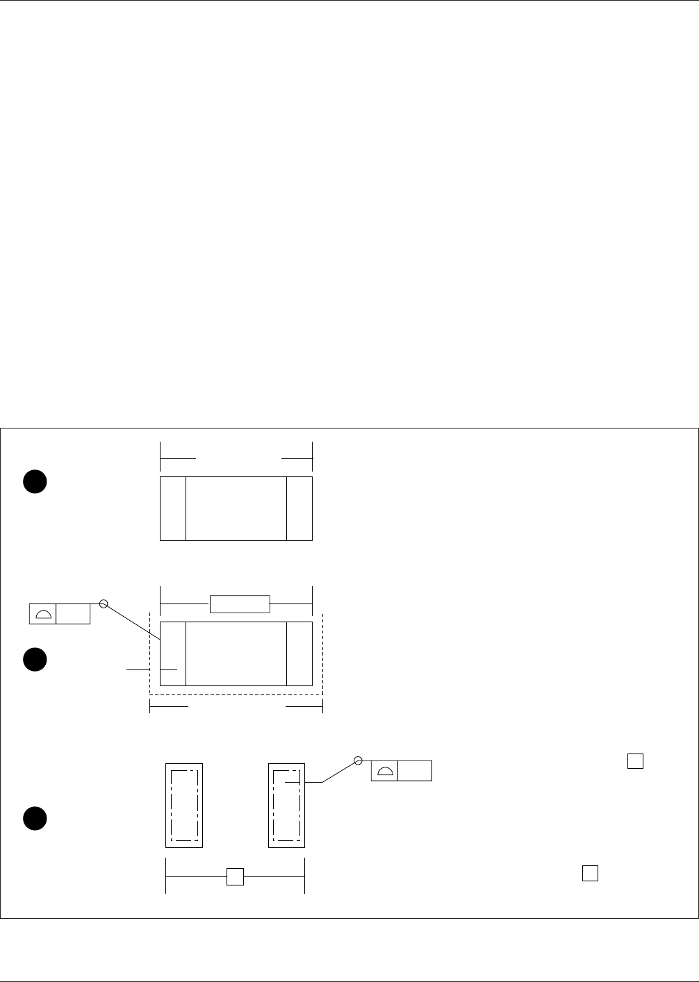
As an example, capacitor C3216 has a manufactured nomi-
nal dimension for its length of 3.2 mm. The tolerance
described by the manufacturer is ± 0.2 mm. Thus, the mini-
mum dimension of ‘‘L’’ is 3.0 mm with a unilateral toler-
ance of 0.4 mm, resulting in its maximum dimension being
3.4 mm.
Figure 3-2 shows the characteristics for the 3216 capacitor.
Item A in Figure 3-2 shows the component manufacturer’s
dimensions for the length of the capacitor. Item B in Fig-
ure 3-2 shows the component length at its minimum size in
the converted dimensions of the new system using profile
tolerancing. Item C in Figure 3-2 shows the land pattern at
its maximum size. These conditions provide for an opti-
mum toe fillet. For optimum heel fillet, the component
basic dimensions are at the maximum and the land pattern
is at its minimum.
Similar concepts are applied to leaded surface mount parts.
The critical dimensional characteristics identified are those
that relate to the formation of the toe and heel solder fillet.
For components with gull-wing leads, the basic dimensions
apply across the outer extremities of the part for toe land
projection; and within the inside of the formed radius of
opposing leads for heel solder fillet formation.
The outer dimensions of leaded or even leadless chip car-
riers are usually easy to determine since these are readily
available from the component manufacturer or standards
organization. The inner (heel-to-heel) dimensions are not
provided in industry standards or manufacturers’ specifica-
tions and are more difficult to determine, not only because
of the form of the lead, termination, or castellation but also
because the inner dimensions must be derived by subtract-
ing the sum of the dimensions of the leads (with all their
inherent tolerances) from the overall dimensions of the
part.
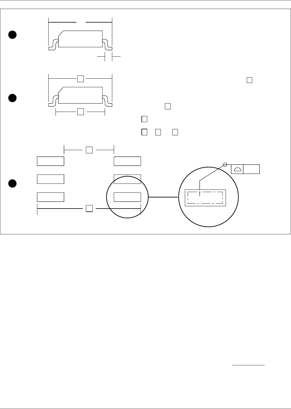
Item A in Figure 3-3 shows the concept for the manufac-
turer’s dimensions and tolerances for a gull-wing SOIC.
Item B in Figure 3-3 shows the converted dimensions to be
considered in the overall mounting system requirements.
IPC-7351-3-02
Figure 3-2 Example of 3216 (1206) Capacitor Dimensioning for Optimum Solder Fillet Condition
3.2 ± 0.2 mm
▼
▼
▼
▼
3.0 LMC
▼
0.2
▼
▼
Maximum
Component Size
▼
▼
Z
MMC
▼
▼
▼
▼
0.05
Manufacturers dimensions
and tolerances (maximum
length of part is 3.4 mm).
Part shown with length at
"least material condition,"
and profile tolerance to
indicate maximum range of
component length at 3.4 mm.
Land pattern with dimension Z
at "maximum material condition."
Profile tolerance of part (0.2 X 2),
plus profile tolerance of land pattern
(0.05 X 2) plus placement accuracy
(0.1 diameter of true position) are
considered in determining the
proper dimension for Z , plus
the desired toe fillet.
A
B
C
February 2005 IPC-7351
7
www.bzfxw.com
Item C in Figure 3-3 shows the land pattern dimensions.
The basic dimensions define the minimum length as mea-
sured across the two outer extremities. As component tol-
erances for ‘‘L’’ increase the maximum length, the oppor-
tunity for the toe fillet is subsequently reduced.
The inner dimensions between heel fillets on opposing
sides are the most important. Inner dimensions are derived
by:
a. Establishing the maximum outline of the component as
measured from lead termination end to lead termination
end. (This dimension is shown as ‘‘L,’’ and is provided
by the manufacturer).
b. Establishing the minimum amount of the lead length as
measured across the ‘‘footprint’’ (from heel to toe for
gull-wing leads). (This dimension is ‘‘T,’’ and is pro-
vided by the manufacturer).
c. Subtracting twice the minimum lead length of (T) from
the maximum overall component length of (L) to arrive
at the maximum length inside the leads across the length
of the component (the inner dimension between oppos-
ing heel fillets). Including the tolerances on dimensions
(L) and subtracting the maximum dimension of T x 2
will yield the minimum dimension between opposing
heels. This signifies worst- case tolerance analysis.
d. Three sets of tolerances are involved in the analysis
described within three tolerances on the overall compo-
nent, plus the tolerances for the lead on each end. Since
not all three tolerances are considered at their worst
case, a recommended method for determining the statis-
tical impact is to summarize the squares of the toler-
ances and take the square root of their sum as the RMS
(root-mean-square) tolerance difference.
For example,
RMS tolerance accumulation =
√
(L
tol
)
2
+ 2(T
tol
)
2
Where:
L
tol
=L
max
-L
min
T
tol
=T
max
-T
min
IPC-7351-3-03
Figure 3-3 Profile Dimensioning of Gull-Wing Leaded SOIC
L
▼
▼
▼
▼
T
L
▼
▼
S
MMC
▼
▼
G
▼
▼
▼
Z
▼
▼
▼
0.05
"
N
"
Places
Fabrication
tolerance
equals 0.1 mm.
Manufacturers dimensions and tolerances
converted to profile dimensions, with S
at "maximum material condition."
Note: If S is not provided by the component
manufacturer it may be determined by subtracting
T terminal dimensions from the length.
S = L - 2 T
Manufacturing dimensions of SOIC's.
A
B
C
MMC MMC LMC
IPC-7351 February 2005
8
标准分享网 www.bzfxw.com 免费下载