IPC-7351-2005_表面贴装焊盘布局设计和标准通用要求.pdf - 第35页
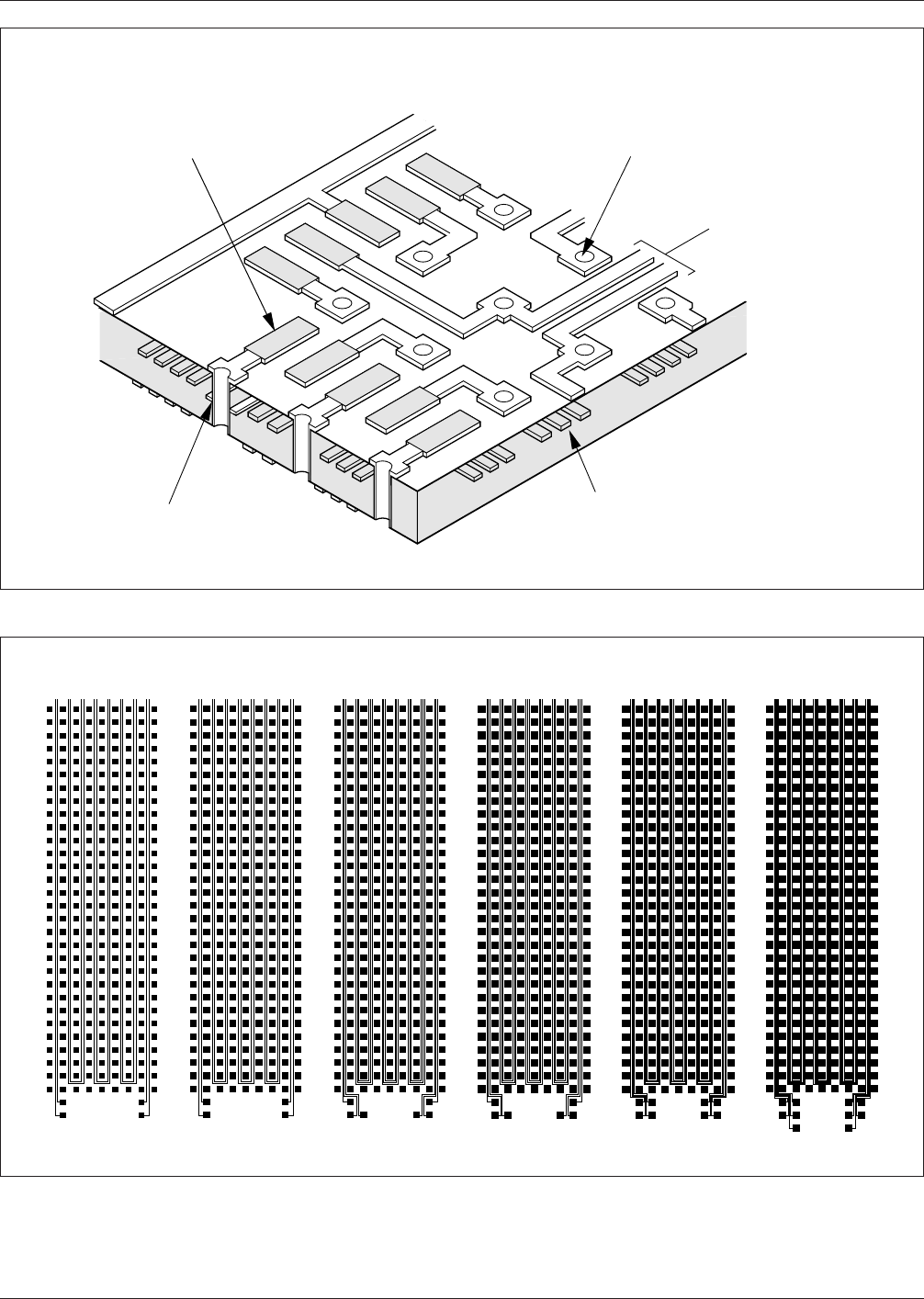
www.bzfxw.com IPC-7351-3-12 Figure 3-12 Use of Vias in High Component Density Printed Circuit Boards Surface Mount Componant Land Pattern Internal Connection Plated via for interface between the outer circuit layer and s…

www.bzfxw.com
the fiducial mark is 1.0 mm. The maximum diameter of the
mark is 3.0 mm. Fiducial marks should not vary in size on
the same PCB more than 25 µm. A clear area devoid of any
other circuit features or markings shall exist around the
fiducial mark. The minimum size of the clear area shall be
equal to twice the radius of the mark (see Figure 3-11).
3.4.4.4 Zonal Fiducials To ensure the accurate place-
ment of multiple surface mount components that are not
near ‘component specific local fiducials’ or ‘global fidu-
cials’, additional ‘zonal fiducial targets’ may be placed
within a zone or an area of the board assembly to compen-
sate for board dimensional stability.
3.4.4.5 Material The fiducial mark may be bare copper,
bare copper protected by organic coating or metal plating.
If solder mask is used, it should not cover the fiducial mark
or the clearance area. It should be noted that excessive oxi-
dation of a fiducial mark’s surface may degrade its read-
ability.
3.4.4.6 Flatness The flatness of the surface of the fidu-
cial mark should be within 15 µm.
3.4.4.7 Edge Clearance The edge of the fiducial should
be no closer to the board edge than the sum of 4.75 mm
and the minimum fiducial clearance required. If less than
this sum, a board handling fixture may be required.
3.4.4.8 Contrast Best performance is achieved when a
consistent high contrast is present between the fiducial
mark and the PCB base material.
The background for all fiducial marks must be the same.
That is, if solid copper planes are retained under fiducials
in the layer below the surface layer, all fiducials must retain
uniform background. If copper is clear under one fiducial,
all must be clear.
3.4.5 Conductors
3.4.5.1 Conductor Width and Spacing
Increased com-
ponent density on SMT designs has mandated the use of
thinner copper, narrower conductor width and spacing.
Higher component density may increase PCB layer counts
as well, requiring the use of more vias to make the neces-
sary connections between layers (see Figure 3-12).
3.4.5.2 Inner Layer Conductors The use of wider con-
ductors and spacing often drives layer counts up because
there is less routing channel available between vias. It is
for this reason that there is an increased usage of narrower
conductors on internal layers. Figure 3-13 compares the
number of routing channels available between lands using
the 0.15 mm geometry. Since conductor width control is
much more difficult to maintain on outer layers of the PCB,
it is better to keep the narrower conductor geometries on
the inner layers of a multilayer printed board. Generally,
the option of using narrow geometries is driven by the need
to reduce layer counts. Decreasing layer counts may reduce
the overall board thickness and improve the aspect ratio for
small hole drilling.
3.4.6 Via Guidelines
3.4.6.1 Drilled Via Holes
The size of the via holes
should be selected on the basis of the printed board thick-
ness versus the hole diameter or aspect ratio limits as
defined by the printed board fabricator. In addition, specific
via lands and holes can be accessed for automatic in-circuit
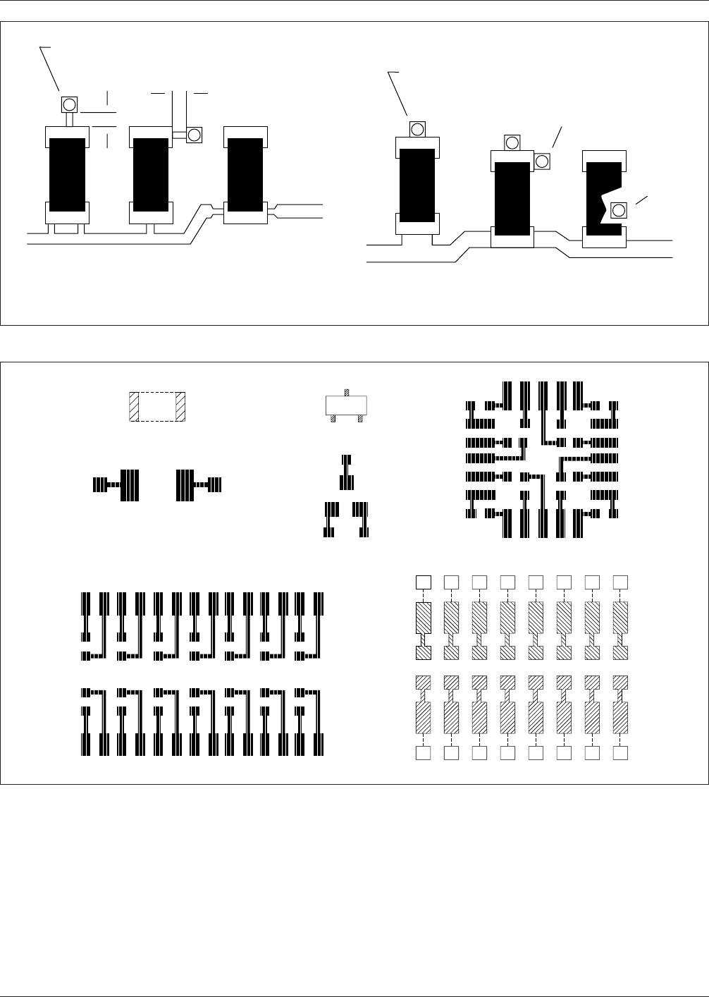
test (ICT). Figure 3-14 shows the land-pattern-to-via rela-
tionships.
3.4.6.2 Vias and Land Pattern Separation For reflow
soldering, via lands must be located away from the compo-
nent lands to prevent solder migration. This migration will
cause insufficient solder fillets on components. The solder
migration can be restricted by providing a narrow conduc-
tor between the land area and the via or prevented by using
the soldermask over bare copper circuitry. The relationship
for mounting land and via locations should consider the
conductor routing requirements. Figure 3-15 provides sev-
eral examples of via positioning concepts.
Wide conductors connecting to a land area can act as a sol-
der thief by drawing solder away from the land and down
the conductor. Furthermore, if the conductor goes to a via
which is connected to an inner layer power or ground
plane, the plane may act as a heat sink and draw heat away
from the land/lead area during reflow solder resulting in a
defective solder joint.
Specifying soldermask tented or filled vias will prevent
solder migration on assemblies manufactured with a solder
reflow process. Filled or tented vias also take care of poten-
tial flux entrapment problems under components and are
highly desirable for attaining good vacuum seal during
in-circuit bed-of-nails testing. Tenting is typically done
with a dry film type of soldermask, or if via holes are very
small, may be plugged and tented using liquid soldermask.
IPC-7351-3-11
Figure 3-11 Fiducial Size and Clearance Requirements
R
2R
Clearance
Minimum
▼
▼
▼▼
IPC-7351 February 2005
24
标准分享网 www.bzfxw.com 免费下载
www.bzfxw.com
IPC-7351-3-12
Figure 3-12 Use of Vias in High Component Density Printed Circuit Boards
Surface Mount
Componant Land Pattern
Internal Connection
Plated via for interface
between the outer circuit
layer and subsurface layer
or layers of the board.
External Surface
Routed Circuits
Internal Subsurface
Route Circuit Layer
IPC-7351-3-13
Figure 3-13 Conductor Routing Capability Test Pattern
2 Channel 2 Channel 3 Channel 3 Channel 4 Channel 5 Channel
February 2005 IPC-7351
25
www.bzfxw.com
3.4.6.3 Vias Under Components During wave soldering
of the assembly, flux may potentially become trapped
under zero clearance devices. If the assembly is to be wave
soldered, via holes underneath zero clearance components
on the primary side should be avoided on boards unless
vias are tented with soldermask. Untented via holes may be
located underneath zero clearance surface mount packages
in reflow soldered surface mount assemblies that will not
be exposed to wave soldering (see Figure 3-16).
3.4.6.4 Vias Within Lands Via holes within the surface
mount component attachment lands are permitted only if
the via is plated closed, filled or plugged and capped
(plated) in such a way as to prevent solder migration dur-
ing the component attachment process. A blind or plated
closed micro-via in the land is typically acceptable for sol-
der attachment of surface mount components. Refer to
IPC-2226 for minimum annular ring requirements for
microvias.
IPC-7351-3-14
Figure 3-14 Land Pattern to Via Relationship
▼
▼
▼
▼
▼
Square land
0.50 mm
[0.020 in] min
Chip Components and Feed Through Via Holes
0.50 mm
[0.020 in] min
Good Design
Poor Design
Feed through lands flush against contact area
▼
▼
▼
Too close
to contact
area
IPC-7351-3-15
Figure 3-15 Examples of Via Positioning Concepts
Side 2
Vias
Side 1
Vias
Side 1
Vias
Side 2
Vias
Chip Component
Chip Component
PLCC
SOIC
SOIC
IPC-7351 February 2005
26
标准分享网 www.bzfxw.com 免费下载