IPC-7351-2005_表面贴装焊盘布局设计和标准通用要求.pdf - 第45页
5.7 Printed Board Test Characteristics 5.7.1 Test Land Pattern Spacing Design for testability is as much a part of the schematic design process as it is a part of the board layout process. Ideally , the printed board wou…
in the test fixture. The test system can then drive each
device on the assembly and quickly locate defective
devices or identify assembly process problems.
To insure precise alignment of the probe contact pins with
the printed board, exact x and y probe position and specific
networks must be furnished to the fixture developer. Iden-
tifying the test locations as components in the CAD data-
base will allow for easy transfer of fixture drilling data.
This data will reduce fixture development time and elimi-
nate the drilling of excessive, nonfunctional holes in the
fixture base. For low volume assembly, or high component
density assembly, fixtureless testing by way of flying probe
equipment is an option.
5.3.2 Multi-Probe Testing Some test probe systems can
exert considerable deformation forces on the assembled
boards and are a known source of premature service fail-
ures. An essential part of the printed board layout is to
ensure that the location of probing points on the board are
staggered at sufficient distances to avoid excessive defor-
mation during multi-probe testing. When the probe point
locations are highly concentrated, additional support may
be needed in the test fixture design in order to counter the
effect against the high probe pressure concentration. The
area on the board where the support is to be provided
should be located where it is clear of conductors and com-
ponents.
5.4 Limited Nodal Access Provided the designer has
allowed sufficient room for access to the test land(s), lim-
ited nodal access (less than 100%) still allows the use of
spring probe (bed-of-nails) testing, but not as effectively as
full nodal access does. When nodal access is less than
100%, shorts, defects and in-circuit testing cannot be per-
formed completely, and some faults may not be detected.
A greater burden is therefore placed on functional or sys-
tem test to detect and diagnose shorts, defects, and bad
devices. This burden varies inversely with the nodal access
percentage. The extra effort at functional test may consist
of additional recurring manpower cost to diagnose failing
boards, or it may mean developing a more detailed func-
tional test (nonrecurring cost) than would have been
planned otherwise.
5.5 No Nodal Access No nodal access (0%) prohibits
bed-of-nails testing and defers all assembly defects and
component testing until the functional or system test bed.
This can only be cost-justified if the much higher cost-per-
defect repair is performed so infrequently that the total cost
is less than the cost of developing and operating an ATE
bed-of-nails test. In other words, the first pass yields must
be extremely high to justify this approach.
5.6 Clam-Shell Fixtures Impact Probing the printed
board from both sides requires a ‘‘clam-shell’’ type of fix-
ture. These are expensive, take more time to fabricate,
require larger test lands on the primary side to protect
against registration problems due to tolerance stack-ups,
and they are more difficult to maintain.
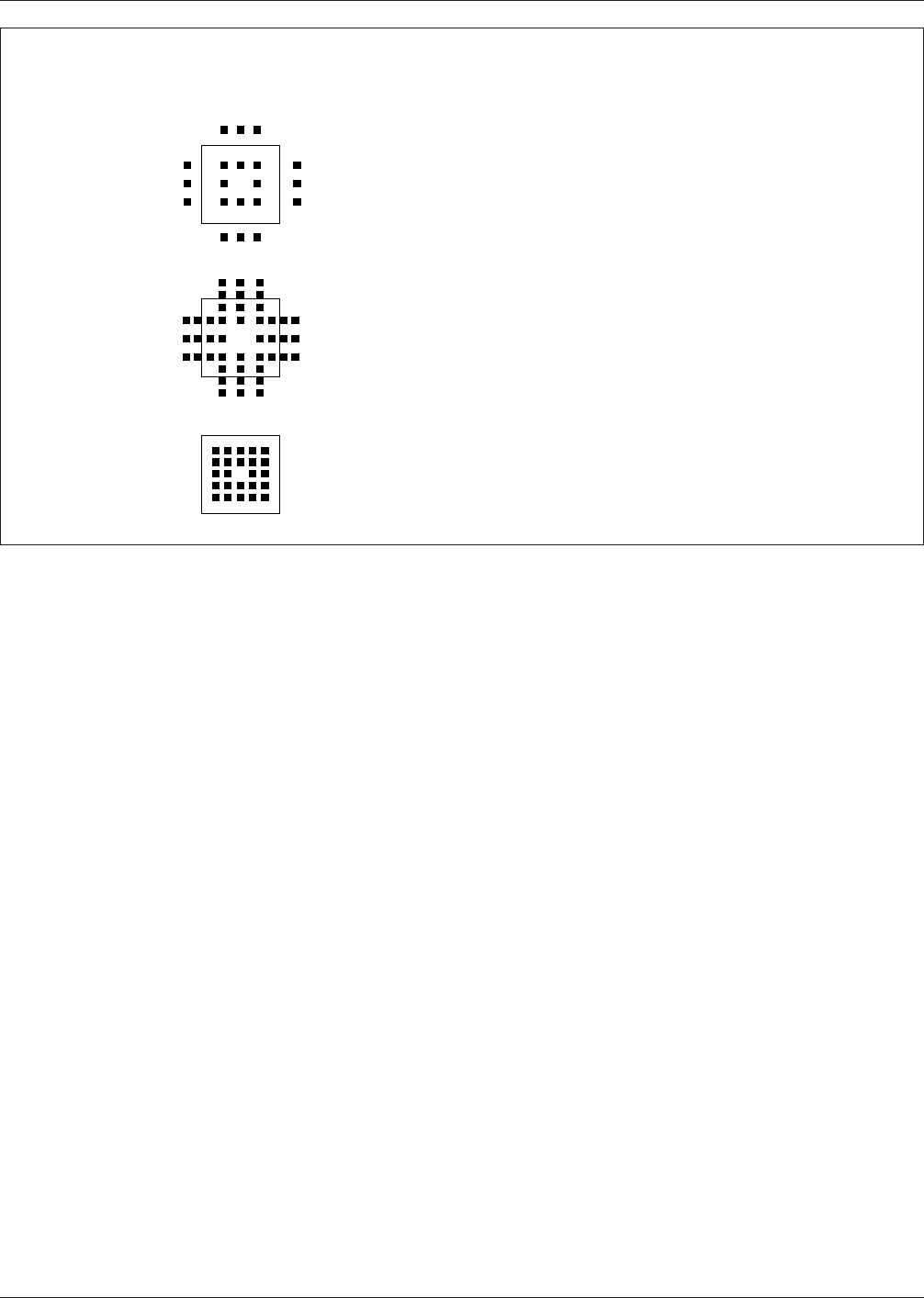
IPC-7351-5-01
Figure 5-1 Test Via Grid Concepts
Test Via Grid Concepts
1.25 mm Pitch Component
2.5 mm Via Test Grid
1.25 mm Pitch Component
1.25 mm Via Test Grid
0.63 mm Pitch Component
1.25 mm Via Test Grid
Preferred
Acceptable
Poor Design
IPC-7351 February 2005
34
标准分享网 www.bzfxw.com 免费下载
5.7 Printed Board Test Characteristics
5.7.1 Test Land Pattern Spacing
Design for testability
is as much a part of the schematic design process as it is a
part of the board layout process. Ideally, the printed board
would have 100% of the nodes accessable from the second-
ary side of the PB assembly. In-circuit testers must have
access to at least one node per net. Probe spacing is
optional; however, standard probe spacing is typically
2.0 mm [0.0787 in] to 2.5 mm [0.0984 in] while miniature,
needle type probes can be spaced as close as 1.0 mm
[0.0394 in] to 1.25 mm [0.04921 in].
The drawbacks to the 1.0 mm [0.0394 in] to 1.25 mm
[0.04921 in] grid-based test lands are the following. The
miniature, needle type probes are more expensive and they
do not hold up as well in high-volume production. Also,
any via sites that are to be used as test points should be
solder filled for better contact and increased probe life.
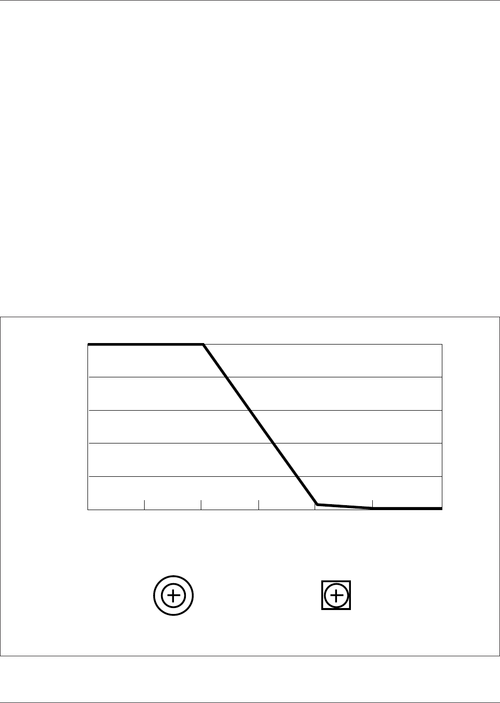
5.7.2 Test Land Size and Shape Lands or vias should be
0.9 mm [0.0354 in] to 1.0 mm [0.0394 in] for probing. As
land sizes decrease, misses increase dramatically as shown
in Figure 5-2. The use of square via lands may provide a
larger target zone for the test probe to contact.
5.7.3 Design for Test Parameters The following other
considerations are important to the general land pattern
design that should be incorporated into the printed board.
a) Two unplated tooling holes should be available on
diagonal corners of the printed board.
b) Test lands should be 2.5 mm [0.0984 in] minimum from
the edge of the printed board to facilitate gasketing on
vacuum fixtures.
c) When using vias for test points, caution should be taken
to insure that signal quality is not degraded at the
expense of testing capability.
d) Test lands should be 0.63 mm [0.0248 in] minimum
from mounting land areas.
e) Where possible, provide numerous test lands for power
and ground.
f) Where possible, provide test lands for all unused gates.
Free running gates sometimes cause instability during
in-circuit testing. This will provide a means of ground-
ing these spurious signals.
It is sometimes desirable to provide drive and sense nodes
test lands to perform six-wire bridge measurements during
IPC-7351-5-02
Figure 5-2 General Relationship Between Test Contact Size and Test Probe Misses
Probability of at Least One Miss
Test/Via Probe Contact Size
100%
80%
60%
40%
20%
0%
0.25 mm 0.35 mm 0.5 mm 0.6 mm
Diameter
0.75 mm
0.9 mm
1.0 mm
1.0 mm Dia
[0.04 in]
0.9 mm Square
[0.036 in]
**
*
*
*
February 2005 IPC-7351
35
in-circuit test. Directions for this should come from test
engineering.
In addition, it is useful to identify the test vias and lands on
an assembly drawing in event of the need to modify the
circuit topology. Changes made without moving test lands
avoid fixture modification, saving cost and time.
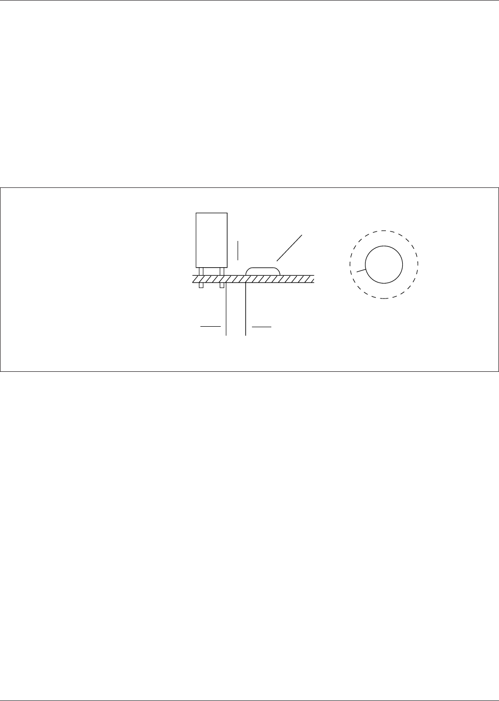
Care should be taken when mounting components on the
secondary side to avoid covering a via hole that is a desig-
nated test land. Also, if a via hole is too close to any com-
ponent, damage may result to the component or fixture
during probing (see Figure 5-3).
6 PRINTED BOARD STRUCTURE TYPES
The selection of a packaging and interconnecting structure
for surface mounting applications is important for optimum
thermal, mechanical and electrical systems reliability. Each
candidate structure has a set of properties with particular
advantages and disadvantages when compared to others
(see Table 6-1).
It is probable that no one packaging and interconnecting
structure or printed board will satisfy all of the needs of the
application. Therefore, a compromise of properties should
be sought that offers the best ‘‘tailoring’’ for component
attachment and circuit reliability.
IPC-7351-5-03
Figure 5-3 Test Probe Feature Distance from Component
Component
Height
▼
▼
▼
Free
Area
6.5 mm [0.256 in] height
> 5.0 mm
[0.20 in] Min.
Test
Pad
5.0 mm [0.20 in]
Tall Component
Free area
▼
▼
Test Pad
IPC-7351 February 2005
36
标准分享网 www.bzfxw.com 免费下载