IPC-7351-2005_表面贴装焊盘布局设计和标准通用要求.pdf - 第53页
latent heat is released as the vapor condenses on the part to be soldered. The soldering temperature is constant and is controlled by the type of fluid. Unlike wave, IR, convection and laser soldering, vapor phase solderi…

Each surface mount device is aligned using the body cen-
ter and a starting orientation for reference. ‘‘0’’ degree is
the basic orientation of the device.
Rotational data must be specified from the ‘‘0’’ position in
a counter-clockwise direction (typically 90°- 180 - 270).
The ‘‘0’’ starting position of the component is significant.
Tape and reel and JEDEC tray packaged devices for
example, have an established standard for orientation.
The tape-and-reel packaged devices have a predetermined
orientation that is related to the perforated pattern on one
edge of the embossed tape carrier. The standard orientation
does vary, however, between unique device families.
Passive and active devices are supplied in a tape and reel
format, held and protected within an embossed pocket.
Each device family or package type has a standard orienta-
tion in relation to the perforated indexing pattern at the
tape edge.
Orientation as well as polarity of a device must be defined
in the CAD database if the output transferred to assembly
systems is to be reliable. Resistors and capacitor devices
are common in orientation and have no defined polarity. As
the designer develops the component database, numbers
are typically assigned to each end of the device to accom-
modate circuit routing and maintain orientation of value
marking or polarity. Tantalum capacitors, diodes, ICs and
other polarized components, for example, have unique ori-
entation in relation to tape feed systems. Consider the rela-
tionship of the device orientation within the tape cavity to
perforation at the tape carrier material edge.
7.4 Soldering Processes Like the selection of auto-
mated placement machines, the soldering process selection
depends upon the type of components to be soldered and
whether or not they will be used in combination with
leaded parts. For example, if all components are surface
mount types, reflow method (vapor phase, hot air convec-
tion or infrared) may be desirable. However, for through-
hole and surface mount combinations, in mixed technology,
a combination of wave soldering and reflow soldering may
be used. No process is best for all soldering tasks. In addi-
tion, the number of soldering processes discussed in the
following text are by no means complete.
7.4.1 Wave Soldering Wave soldering is an economical
method of soldering mass terminations. There are five to
six main process variables that must be controlled in the
wave soldering process: fluxing, preheat, conveyor speed,
conveyor incline, solder temperature, and possibly cooling
rate.
In preheat, allowance in the conveyer system must be made
for the thermal expansion of the board during preheating
and soldering to prevent board warpage.
In fluxing, flux density, activity and flux foam/flux spray/
flux wave height must be closely monitored. A system must
be in place to determine when the flux activity has deterio-
rated and when the old flux must be replaced and the new
flux added.
Speed is the time sequence and duration of all of the steps
in soldering. By controlling the speed, more uniform and
better joints result. In controlling the conveyer speed, pre-
heating a packaging and interconnecting assembly in two
or three stages minimizes the thermal shock damage to the
assembly and improves its service life. Uniform preheating
is achieved by developing a solder schedule that specifies
preheat settings and conveyer speed for each type of board.
The solder wave is an important variable. Wave geometry
is especially important for preventing icicles and bridges
and for the proper soldering of surface mounted compo-
nents. Wave geometries include uni-directional and
bi-directional; single and double; rough, smooth and dead
zone; oil intermix, dry, and bubbled, and with or without a
hot air knife. Special solder waves just for surface mounted
components are also available.
The concern generally expressed in wave soldering of sur-
face mount devices is damage to the components when
they go through the soldering wave at 260 °C [500 °F]. The
maximum shift in tolerance of resistors and capacitors is
generally found to be 0.2%. This is a negligible amount
considering the part tolerance of commonly used compo-
nents is 5% to 20%. The components generally spend about
three seconds in the wave but they are designed to with-
stand soldering temperatures of 260 °C [500 °F] for up to
ten seconds.
In wave soldering, outgassing and solder skips are two
other main concerns. The outgassing or gas evolution
occurs on the trailing terminations of chip resistors and
capacitors. It is believed to be caused by insufficient drying
of flux and can be corrected by raising the packaging and
interconnecting assembly preheat temperature or time. The
other concern, solder skips, is caused by the shadow effect
of the part body on the trailing terminations. Orienting the
part in such a way that both terminations are soldered
simultaneously solves most shadow effect problems. Some
manufacturers use an extra land to serve as a ‘‘solder
thief’’ for active components.
The most common method for solving both outgassing and
shadow effect is by switching to the dual wave system
where the first wave is turbulent and the second wave is
laminar. The turbulent wave serves to provide an adequate
amount of solder across the surface of the packaging and
interconnecting structure in order to help eliminate outgas-
sing and solder skips. The laminar wave is used to help
eliminate icicles and bridging.
7.4.2 Vapor Phase (VP) Soldering Vapor phase solder-
ing, also known as condensation soldering, uses the latent
heat of vaporization of an inert liquid for soldering. The
IPC-7351 February 2005
42
标准分享网 www.bzfxw.com 免费下载

latent heat is released as the vapor condenses on the part to
be soldered. The soldering temperature is constant and is
controlled by the type of fluid.
Unlike wave, IR, convection and laser soldering, vapor
phase soldering does not require control of the heat input
to the solder joints or to the board. It heats independently
of the part geometry, heats uniformly, and does not exceed
the fluid boiling temperature. This process is also suitable
for soldering odd-shaped parts, flexible circuits, and pins
and connectors, as well as for reflow of tin-lead electro-
plate and surface mount packages. Since heating is by con-
densation, the rate of temperature rise depends on the mass
of the part. Therefore, the leads on the package in contact
with the packaging and interconnecting structure heat up
faster than the component body. This may lead to wicking
of the solder up the lead. Before exposing the loaded
assembly to VP reflow process, preheating the assembly is
highly recommended to avoid thermal shock to compo-
nents and the PCB.
7.4.3 IR Reflow Soldering
In infrared (IR) reflow soldering, the radiant or convective
energy is used to heat the assembly. There are basically two
types of IR reflow methods, either focused (radiant) or
nonfocused (convective). The latter is proving more desir-
able for SMT. The focused IR radiates heat directly on the
parts and may unevenly heat assemblies. The heat input on
the part may also be color-dependent. In nonfocused or
diffused IR, the heating medium can be air or an inert gas
or simply the convection energy. A gradual heating of the
assembly is necessary to drive off volatiles from the solder
paste. After an appropriate time in preheat, the assembly is
raised to the reflow temperature for soldering and then
cooled.
7.4.4 Hot Air/Gas Convection Soldering The reflow
process affects soldering by transporting the boards through
a stream of heated gas (e.g., air, nitrogen). Heat is trans-
ferred to the components and board by conduction from the
gas. Because the boards do not receive significant direct
radiation from the heating source, convection soldering
avoids the shadowing problems that can occur with infra-
red soldering machines, especially short wavelength (lamp)
versions. This enables more uniform heating and a higher
component density on the board compared to other mass
reflow soldering methods. The gas temperature controls the
maximum temperature that can be seen by the assembly.
Use of a nitrogen atmosphere permits better thermal cou-
pling between the circulating gas and the component termi-
nations. In addition to improved wetting, the process win-
dow for double-sided reflow is enlarged, and lower
activated solder paste flux can be used.
7.4.5 Laser Reflow Soldering Laser soldering comple-
ments other mass soldering processes rather than replacing
them and, as with in-line reflow soldering, lends itself well
to automation. It is faster than hand soldering but not as
fast as wave, vapor, IR soldering or hot air convection.
Heat-sensitive components that may be damaged in reflow
processes can be soldered by laser. Process problems
include thermal damage to surrounding areas and solder
balls.
7.4.6 Conduction Reflow Soldering Conduction reflow
affects soldering through the transference of heat from
beneath the PCB. This can have advantages with high mass
components, temperature sensitive components and metal
backed assemblies. In comparison with other solder pro-
cesses, the slightly slower heating and cooling ramp times
caused by heat spreading through the PCB substrates can
provide a reduction of thermal shock and improved resis-
tance against rapid cooling issues such as tombstoning.
Though in-line conduction reflow ovens are available, the
most common use of conductive reflow is in ‘‘hot plate’’
rework systems.
For more detail regarding reflow soldering refer to IPC-
7530.
7.5 Cleaning Flux requiring solvent cleaning—synthetic
or rosin-based fluxes are generally known as synthetic acti-
vated (SA), synthetic mildly activated (SMA), rosin acti-
vated (RA) or rosin mildly activated (RMA). Stabilized
halogenated hydrocarbon/alcohol azeotropes are the pre-
ferred solvents for removal of synthetic and rosin-based
flux residues.
7.6 Repair/Rework The repair/rework of surface mount
assemblies requires special care in design and practice.
Because of the small land geometries, heat applied to the
board should be minimized. There are various tools avail-
able for removing components. Resistance heating twee-
zers are usually used for removing surface mounted com-
ponents. Various types of hot air/gas and IR systems are
also used for removing surface mounted components. One
of the main issues when using hot air/gas devices is pre-
venting damage to adjacent components. Refer to IPC-
7711/21. There are four basic requirements for a successful
rework; good printed board design layout, selection of the
correct rework equipment or tools, sufficient manual skill,
and adequate training.
Successful removal of large multi-leaded integrated circuit
packages involves the use of hot gas or heated electrode
tools. Sufficient clearance around the package to permit the
re-work is essential. Clearance should be provided com-
pletely around the device as identified in the standards as
the ‘‘courtyard manufacturing zone.’’
7.6.1 Heatsink Effects Large ground planes or heatsinks
will conduct heat away from the component being
reworked if present in a printed board substrate. Extra heat,
February 2005 IPC-7351
43
perhaps for longer periods, is then required which, in turn,
can lead to damage to components or the board. The fact
that the solder joints may not reach reflow temperature is
no guarantee that the component or the board have not
been overheated. Heatsinking effects is a design problem
which must be tackled at the printed board layout stage.
Whenever possible, any component termination which may
not rework, including leaded-through hole type, should be
thermally isolated from any ground plane or integral heat-
sink by a short length of copper conductor.
7.6.2 Dependence on Printed Board Material Type To
ensure minimum damage to the printed board during
rework, base laminate should be a good quality resin and
reinforcement type from a high copper peel strength mate-
rial. High packing density is required. The use of inferior
laminates can easily lead to problems with lands peeling
away during rework. This may result in either scrapping of
complete assemblies or expensive repair of damaged cop-
per area. For boards having high thermal mass such as
middle-core types or those with large area ground planes,
to avoid employing a tool with high heat input rate, the use
of a hot plate to provide background heating is essential.
7.6.3 Dependence on Copper Land and Conductor Lay-
out
The space on a board is at a premium or single con-
ductors must be kept very short. Designers will often route
a conductor between adjacent device land space at a pitch
of the component device being placed. In such cases, con-
ductors should be covered with a soldermask to minimize
the risk of lifting conductors during rework operations.
Routing conductors between lands at 1.0 mm pitch and
below increases the risk of damage to the conductors dur-
ing the rework operation. For more detail regarding devel-
opment, planning and trouble shooting the steps involved
in the process of producing surface mount assemblies, refer
to IPC-S-816.
8 IPC-7352 DISCRETE COMPONENTS
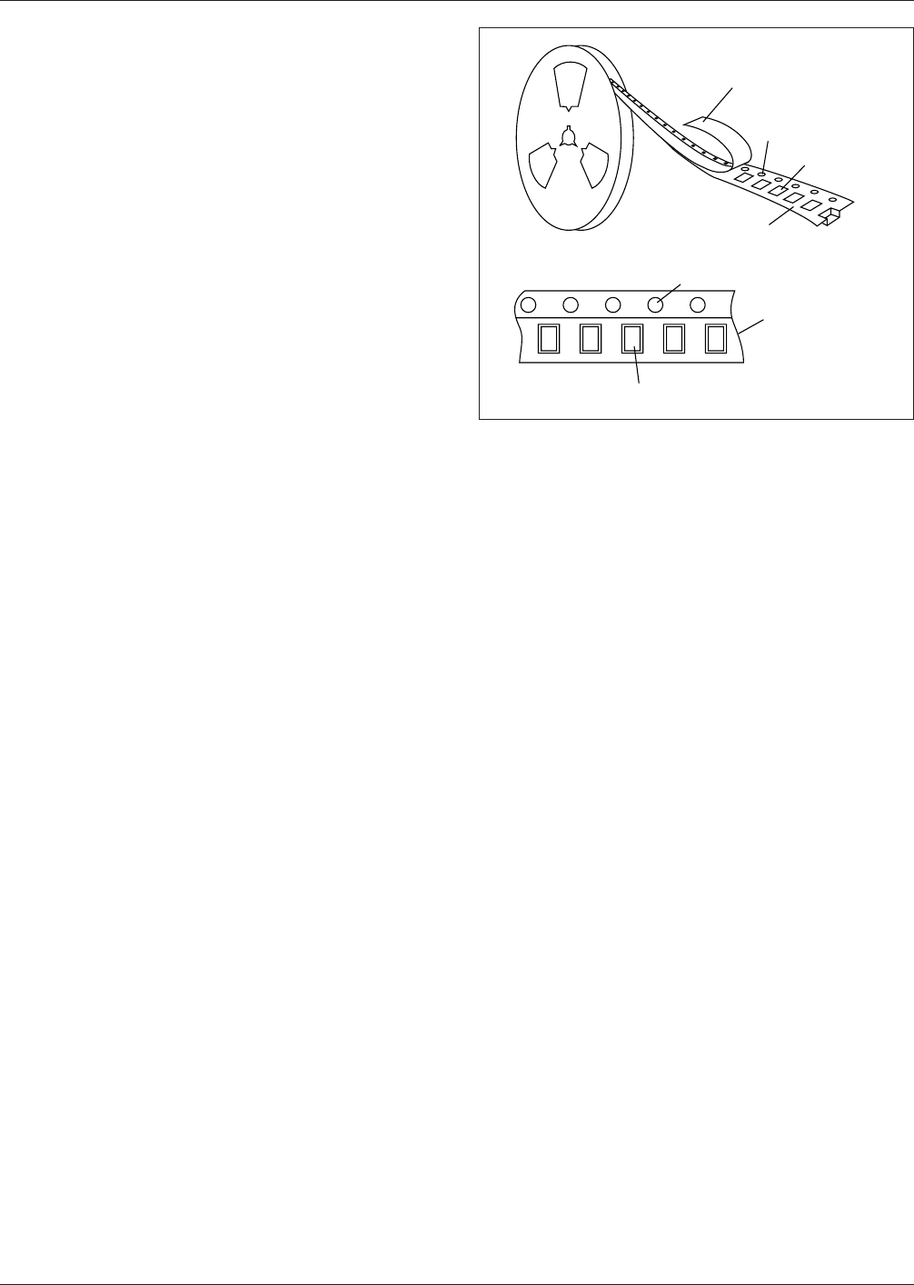
Discrete components are generally purchased in 8 mm and
12 mm wide tape and reel (see Figure 8-1). EIA-481 is the
applicable specification for tape and reel. Consult your
manufacturers guide for the packaging availability of your
component.
Parts susceptible to damage by electrostatic discharge shall
be supplied in a manner that prevents such damage. Tape
peel strength shall be 40 grams ± 30 grams. Peel from the
top for the top cover of the tape. Reel materials used in the
construction of the reel shall be easily disposable metal,
chip board, styrene plastic or equivalent. Reels shall not
cause deterioration of the components or their solderability.
Reels must be able to withstand high humidity conditions.
Parts must be capable of withstanding cleaning processes
currently used by board assembly manufacturers. This may
include as a minimum four-minute exposures to solvent
cleaning solutions at 40 °C [104 °F], plus a minimum of a
one-minute exposure to ultrasonic immersion at a fre-
quency of 40 kHz and a power of 100 watts per square
foot. Alkaline systems in use shall also not damage parts or
remove markings.
End terminations should be solder coated with a tin/lead
alloy or a lead free equivalent. The solder should contain
between 58 to 68% tin. Solder may be applied to the ter-
mination by hot dipping or by plating from solution. Plated
solder terminations should be subjected to a postplating
reflow operation to fuse the solder. The tin/lead finish
should be at least 0.0075 mm [0.0003 in] thick.
The termination shall be symmetrical, and shall not have
nodules, lumps, protrusions, etc., that compromise the sym-
metry or dimensional tolerances of the part. The end termi-
nation shall cover the ends of the components, and shall
extend out to the top and bottom of the component.
Solder finish applied over precious metal electrodes shall
have a diffusion-barrier layer between the electrode metal-
lization and the solder finish. The barrier layer should be
nickel or an equivalent diffusion barrier, and should be at
least 0.00125 mm [0.00005 in] thick.
For lead free finishes a combination of tin, silver and cop-
per is the prevalent replacement for the tin/lead finish. Sol-
derability testing should be applied per IPC-J-STD-002 to
determine attachment capability of the applicable compo-
nent type.
The following sections for each component family provide
information on basic component construction, termination
materials, marking, carrier package format and resistance
to soldering.
8.1 Chip Resistors (RESC) A variety of values exist for
resistors. This section describes the most common types.
IPC-7351-8-01
Figure 8-1 Packaging of Discrete Components
Top Cover
Tape
Sprocket
Hole
Component
Cavity
Embossed Carrier Tape
Sprocket Hole
Embossed
Carrier Tape
Component Cavity
▼
▼
▼
▼
▼
▼
▼
IPC-7351 February 2005
44
标准分享网 www.bzfxw.com 免费下载