IPC-7351-2005_表面贴装焊盘布局设计和标准通用要求.pdf - 第60页
reflow operation to fuse the solder . The tin/lead finish should be at least 0.0075 mm [0.0003 in] thick. The termination shall be symmetrical, and shall not have nodules lumps, protrusions, etc., that compromise the sym- …
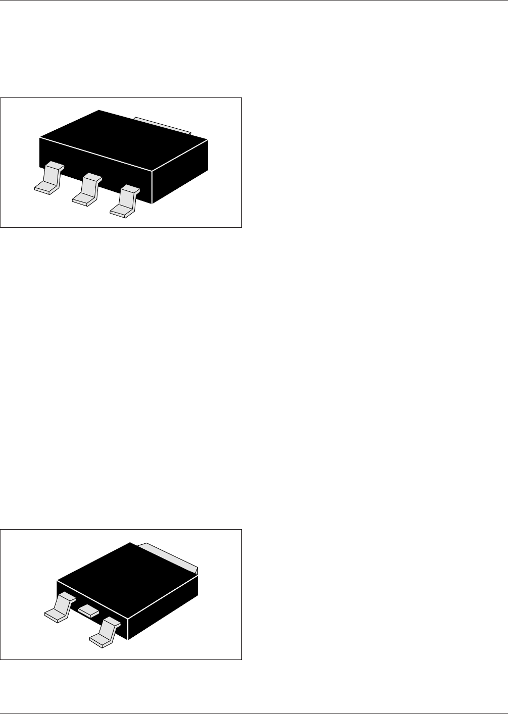
8.10.1 Basic Construction The dimensional characteris-
tics are designed to meet the needs of the surface mount
industry. The clearance between the body of the component
and the packaging and interconnect structure is specified at
0.06 mm [0.00236 in] (basic) to accommodate reflow or
wave soldering processes (see Figure 8-12).
8.10.2 Marking Parts are available with or without
marked values.
8.10.3 Carrier Package Format Carrier package format
shall be according to the following: body type TO-261,
12 mm tape/8 mm pitch.
8.10.4 Resistance to Soldering Parts should be capable
of withstanding five cycles through a standard reflow sys-
tem operating at 215 °C [419 °F]. Each cycle shall consist
of 60 seconds exposure at 215 °C [419 °F]. Parts must also
be capable of withstanding a minimum of 10 seconds
immersion in molten solder at 260 °C [500 °F]. See IPC/
JEDEC J-STD-020 for appropriate reflow cycles and pro-
files when using lead free solders.
8.11 TO252 (DPAK Type) These parts are for dual diodes
and Darlington transistors. IPC-7352 TO252 component
outlines are derived from outline TO-252 ‘‘Issue B’’ within
JEDEC Publication 95.
8.11.1 Basic Construction See Figure 8-13.
8.11.2 Marking Parts are available with or without
marked values.
8.11.3 Carrier Package Format Carrier package format
shall be according to the following: body type TO-252,
12 mm tape/8 mm pitch.
8.11.4 Resistance to Soldering Parts should be capable
of withstanding five cycles through a standard reflow sys-
tem operating at 215 °C [419 °F]. Each cycle shall consist
of 60 seconds exposure at 215 °C [419 °F]. Parts must also
be capable of withstanding a minimum of 10 seconds
immersion in molten solder at 260 °C [500 °F]. See IPC/
JEDEC J-STD-020 for appropriate reflow cycles and pro-
files when using lead free solders.
8.12 Molded Body Diode (DIOSMB)
9 IPC-7353 GULLWING LEADED COMPONENTS, TWO
SIDES
The two-sided gullwing family has a number of generic
package sizes in the family. The body sizes are varied, but
the basic family is characterized by 1.27 mm or 0.63 mm
lead centers with leads on the long side of a rectangular
body. The family has been expanded to include a limited
number of 0.80 mm, 0.65 mm, 0. 50 mm, 0.40 mm, and
0.30 mm pitch devices.
Within the component families, body width and lead span
are constant, while body length changes as the lead count
changes.
A major advantage of this package style is that it can be
pretested prior to substrate assembly while still offering
relatively high density. Its small area, low height, and mini-
mal weight are its major advantages over DIPs. The pack-
age has orientation features on the edge of the package to
aid in handling and identification.
Coplanarity is an issue for all components with gullwings
on two sides. In general, the leads must be coplanar within
0.1 mm. That is, when the component is placed on a flat
surface, (e.g., a granite block), no lead may be more than
0.1 mm off the flat surface.
Note: Some members of the SOIC family are processed on
the secondary side and wave soldered. When parts are pro-
cessed by wave solder, correct part orientation must be
observed. Consult your manufacturer before placing SOICs
on the wave solder side of the board.
High lead count packages and fine pitch parts, 0.63 mm or
less, should be processed by infrared reflow, conduction
reflow, or hot bar soldering, and should not be wave sol-
dered.
End terminations should be solder coated with a tin/lead
alloy or a lead free equivalent. The solder should contain
between 58 to 68% tin. Solder may be applied to the ter-
mination by hot dipping or by plating from solution. Plated
solder terminations should be subjected to a postplating
IPC-7351-8-12
Figure 8-12 SOT 223 Construction
IPC-7351-8-13
Figure 8-13 TO252 (DPAK Type) Construction
February 2005 IPC-7351
49
reflow operation to fuse the solder. The tin/lead finish
should be at least 0.0075 mm [0.0003 in] thick.
The termination shall be symmetrical, and shall not have
nodules lumps, protrusions, etc., that compromise the sym-
metry or dimensional tolerances of the part. The end termi-
nation shall cover the ends of the components, and shall
extend out to the top and bottom of the component.
Solder finish applied over precious metal electrodes shall
have a diffusion-barrier layer between the electrode metal-
lization and the solder finish. The barrier layer should be
nickel or an equivalent diffusion barrier, and should be at
least 0.00125 mm [0.00005 in] thick.
For lead free finishes a combination of tin, silver and cop-
per is the prevalent replacement for the tin/lead finish. Sol-
derability testing should be applied per IPC-J-STD-002 to
determine attachment capability of the applicable compo-
nent type.
9.1 SOIC These small outline integrated circuits (SOIC)
are all on 1.27 mm pitch, and are available in 4.0 mm nar-
row body, 7.50 mm or 7.60 mm wide body and 9.02 mm
extra wide body sizes, ranging from 8 to 36 pins. IPC-7353
SOIC component outlines are derived from outlines
MS-012, MS-013, MO-110 and MO-120 within JEDEC
Publication 95.
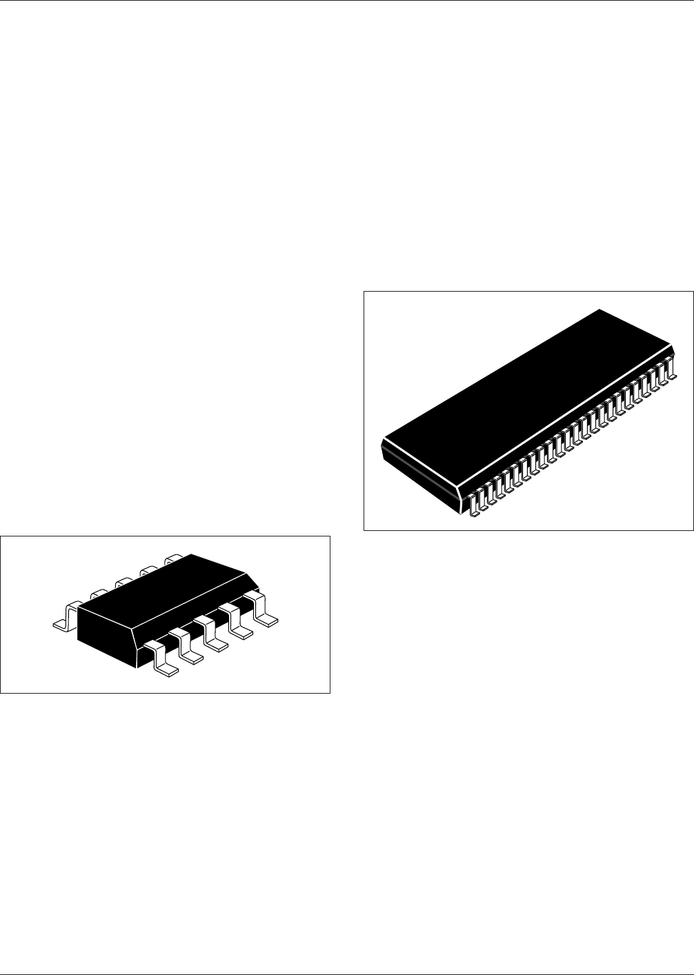
9.1.1 Basic Construction Basic construction consists of
a plastic body and metallic leads (see Figure 9-1).
9.1.2 Marking All parts shall be marked with a part
number and ‘‘Pin 1’’ location. ‘‘Pin 1’’ location may be
molded into the plastic body.
9.1.3 Carrier Package Format Carrier packaging format
may be provided in a tray carrier, but tape and reel carriers
are preferred for best handling and high volume applica-
tions. Bulk packaging is not preferred because of lead
coplanarity required for placement and soldering.
9.1.4 Resistance to Soldering Parts should be capable
of withstanding ten cycles through a standard reflow sys-
tem operating at 215 °C [419 °F]. Each cycle shall consist
of 60 seconds exposure at 215 °C [419 °F]. Parts must also
be capable of withstanding a minimum of 10 seconds
immersion in molten solder at 260 °C [500 °F]. See IPC/
JEDEC J-STD-020 for appropriate reflow cycles and pro-
files when using lead free solders.
9.2 SOP8/SOP63 (SSOIC) These shrink small outline
integrated circuits (SSOIC) are on either 0.635 mm or
0.80 mm pitch, and are available in 7.59 mm wide body
and 12.10 mm extra wide body sizes, ranging from 48 to
64 pins. IPC-7353 SOP8/SOP63 component outlines are
derived from outlines MO-117 Issue ‘‘A’’ and MO-118
Issue ‘‘A’’ within JEDEC Publication 95.
9.2.1 Basic Construction Basic construction consists of
a plastic body and metallic leads (see Figure 9-2).
9.2.2 Marking All parts shall be marked with a part
number and ‘‘Pin 1’’ location. ‘‘Pin 1’’ location may be
molded into the plastic body.
9.2.3 Carrier Package Format Carrier packaging format
may be provided in a tray carrier, but tape and reel carriers
are preferred for best handling and high volume applica-
tions. Bulk packaging is not preferred because of lead
coplanarity required for placement and soldering.
9.2.4 Resistance to Soldering Parts should be capable
of withstanding ten cycles through a standard reflow sys-
tem operating at 215 °C [419 °F]. Each cycle shall consist
of 60 seconds exposure at 215 °C [419 °F]. Parts must also
be capable of withstanding a minimum of 10 seconds
immersion in molten solder at 260 °C [500 °F]. See IPC/
JEDEC J-STD-020 for appropriate reflow cycles and pro-
files when using lead free solders.
9.3 SOP127 (SOP-IPC-782) IPC-7351 has defined
center-to-center spacing for these land patterns slightly dif-
ferently than is indicated in the EIAJ specification EIAJ-
7402-1.
IPC-7351-9-01
Figure 9-1 SOIC Construction
IPC-7351-9-02
Figure 9-2 SOP8/SOP63 Construction
IPC-7351 February 2005
50
标准分享网 www.bzfxw.com 免费下载
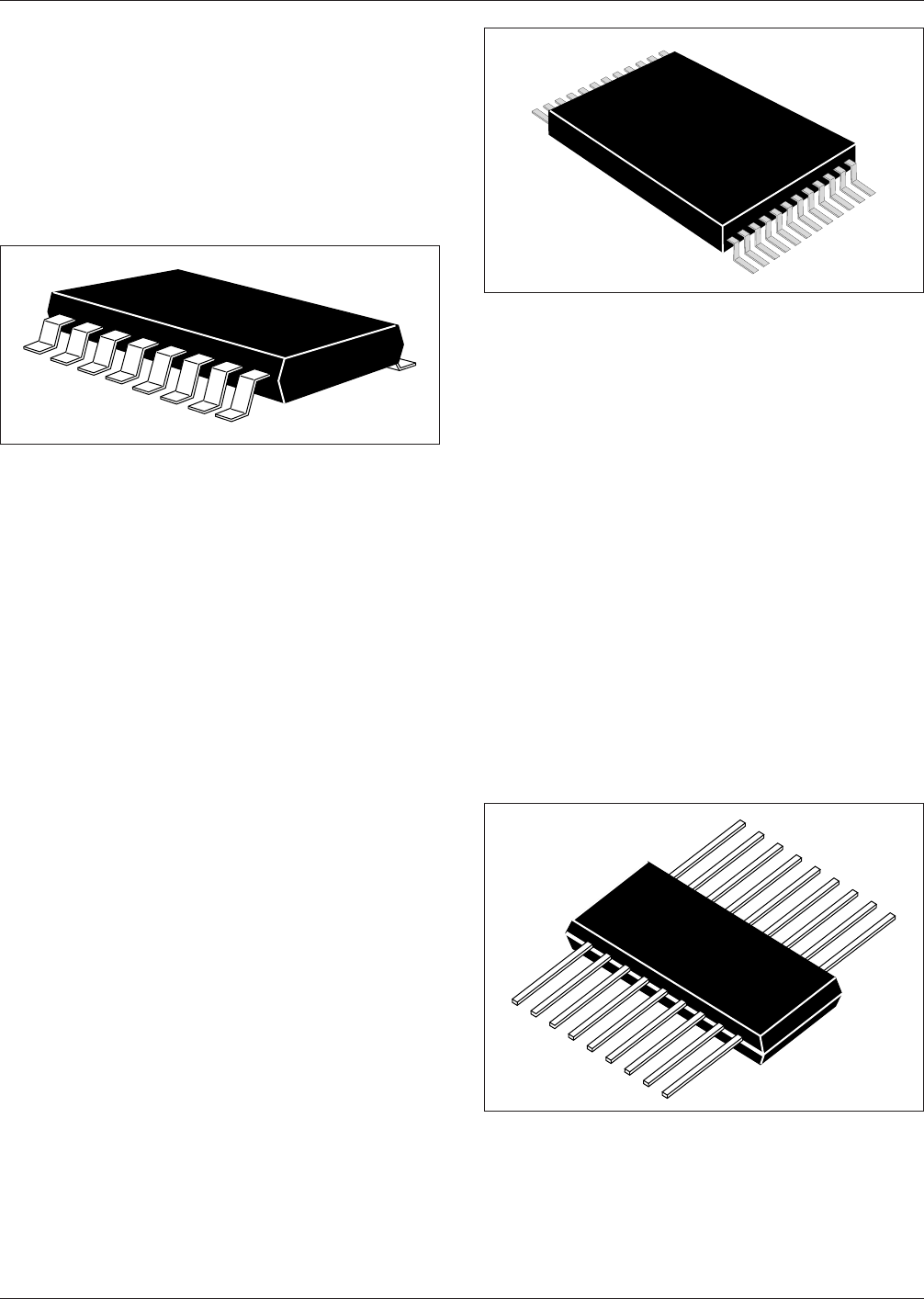
This standard allows for 6 families of the SOP127. EIAJ
classifies the families by the center-to-center distance of
the land patterns and the outer extremities of the leads
(dimension ‘‘L’’ in IPC-7351). The basic construction of
the SOP127 specified by EIAJ is the same construction as
for SOIC specified by JEDEC. Both have gullwing leads
on 1.27 mm centers. The EIAJ specification allows for a
number of positions of the components to be in any of the
families (e.g., body width) (see Figure 9-3).
9.3.1 Marking Parts are available with or without part
number markings. Usually an index mark indicates pin 1.
9.3.2 Carrier Package Format Carrier packaging format
may be provided in a tray carrier, but tape and reel carriers
are preferred for best handling and high volume applica-
tions. Bulk packaging is not preferred because of lead
coplanarity required for placement and soldering.
9.3.3 Resistance to Soldering Parts should be capable
of withstanding ten cycles through a standard reflow sys-
tem operating at 215 °C [419 °F]. Each cycle shall consist
of 60 seconds exposure at 215 °C [419 °F]. Parts must also
be capable of withstanding a minimum of 10 seconds
immersion in molten solder at 260 °C [500 °F]. See IPC/
JEDEC J-STD-020 for appropriate reflow cycles and pro-
files when using lead free solders.
9.4 TSSOPS The thin shrink small outline package
(TSSOP) is unique among the component families of this
section because its leads protrude from the short side of the
plastic body. The TSSOP components are available in four
different pitches: 0.30 mm, 0.40 mm, 0.50 mm, and
0.65 mm. They are typically specified by their two largest
dimensions-the plastic body size (in the short dimension),
and the nominal toe-to-toe length (in the long dimension).
Their use has grown because their height (less than
1.27 mm) allows them to be used in memory card technol-
ogy. IPC-7351 outlines sixteen different body sizes with
pin counts ranging from 16-76 pins. In general, as the long
dimension increases, the pitch decreases (see Figure 9-4).
9.4.1 Marking Parts are available with or without part
number markings. Usually an index mark indicates pin 1.
9.4.2 Carrier Packages Format Trays are usually used
for handling TSSOPs.
9.4.3 Resistance to Soldering Parts should be capable
of withstanding ten cycles through a standard reflow sys-
tem operating at 215 °C [419 °F]. Each cycle shall consist
of 60 seconds exposure at 215 °C [419 °F]. Parts must also
be capable of withstanding a minimum of 10 seconds
immersion in molten solder at 260 °C [500 °F]. See IPC/
JEDEC J-STD-020 for appropriate reflow cycles and pro-
files when using lead free solders.
9.5 CFP127 See Figure 9-5 for an example of a ceramic
flat pack (CFP127). Basic construction consists of a
ceramic body and metallic leads. Leads are trimmed and
formed into gullwing shape and all are on 1.27 mm centers.
IPC-7353 CFP127 component outlines are derived from
outlines MO-003, MO-004, MO-018, MO-019, MO-020,
MO-021, MO-022 and MO-023 within JEDEC Publication
95.
9.5.1 Marking All parts shall be marked with a part
number and an index area. The index area shall identify the
location of pin 1.
9.5.2 Carrier Packages Format Carrier trays are used
for handling CFPs.
IPC-7351-9-03
Figure 9-3 SOP127 Construction
IPC-7351-9-04
Figure 9-4 TSSOP Construction
IPC-7351-9-05
Figure 9-5 CFP127 Construction
February 2005 IPC-7351
51