IPC-7351-2005_表面贴装焊盘布局设计和标准通用要求.pdf - 第18页
www.bzfxw.com Item C in Figure 3-3 shows the land pattern dimensions. The basic dimensions define the minimum length as mea- sured across the two outer extremities. As component tol- erances for ‘ ‘L ’ ’ increase the maxi…
www.bzfxw.com
formation of the acceptable solder joint. Component manu-
facturers usually provide dimensions for their parts with a
nominal size and then put a tolerance on that nominal
dimension. In order to facilitate the dimensioning system,
these dimensions and their associated tolerances are con-
verted to minimum and maximum size.
As an example, capacitor C3216 has a manufactured nomi-
nal dimension for its length of 3.2 mm. The tolerance
described by the manufacturer is ± 0.2 mm. Thus, the mini-
mum dimension of ‘‘L’’ is 3.0 mm with a unilateral toler-
ance of 0.4 mm, resulting in its maximum dimension being
3.4 mm.
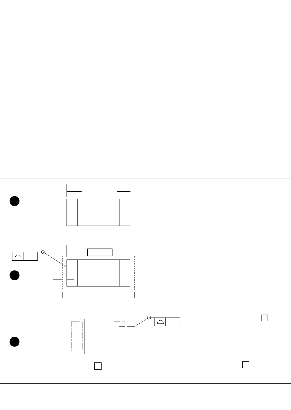
Figure 3-2 shows the characteristics for the 3216 capacitor.
Item A in Figure 3-2 shows the component manufacturer’s
dimensions for the length of the capacitor. Item B in Fig-
ure 3-2 shows the component length at its minimum size in
the converted dimensions of the new system using profile
tolerancing. Item C in Figure 3-2 shows the land pattern at
its maximum size. These conditions provide for an opti-
mum toe fillet. For optimum heel fillet, the component
basic dimensions are at the maximum and the land pattern
is at its minimum.
Similar concepts are applied to leaded surface mount parts.
The critical dimensional characteristics identified are those
that relate to the formation of the toe and heel solder fillet.
For components with gull-wing leads, the basic dimensions
apply across the outer extremities of the part for toe land
projection; and within the inside of the formed radius of
opposing leads for heel solder fillet formation.
The outer dimensions of leaded or even leadless chip car-
riers are usually easy to determine since these are readily
available from the component manufacturer or standards
organization. The inner (heel-to-heel) dimensions are not
provided in industry standards or manufacturers’ specifica-
tions and are more difficult to determine, not only because
of the form of the lead, termination, or castellation but also
because the inner dimensions must be derived by subtract-
ing the sum of the dimensions of the leads (with all their
inherent tolerances) from the overall dimensions of the
part.
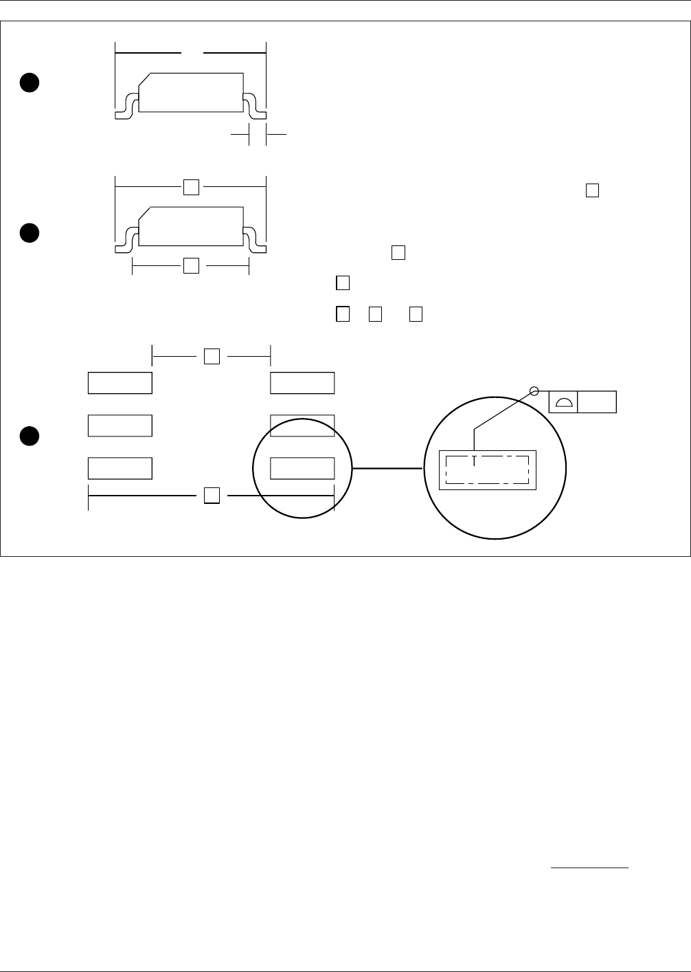
Item A in Figure 3-3 shows the concept for the manufac-
turer’s dimensions and tolerances for a gull-wing SOIC.
Item B in Figure 3-3 shows the converted dimensions to be
considered in the overall mounting system requirements.
IPC-7351-3-02
Figure 3-2 Example of 3216 (1206) Capacitor Dimensioning for Optimum Solder Fillet Condition
3.2 ± 0.2 mm
▼
▼
▼
▼
3.0 LMC
▼
0.2
▼
▼
Maximum
Component Size
▼
▼
Z
MMC
▼
▼
▼
▼
0.05
Manufacturers dimensions
and tolerances (maximum
length of part is 3.4 mm).
Part shown with length at
"least material condition,"
and profile tolerance to
indicate maximum range of
component length at 3.4 mm.
Land pattern with dimension Z
at "maximum material condition."
Profile tolerance of part (0.2 X 2),
plus profile tolerance of land pattern
(0.05 X 2) plus placement accuracy
(0.1 diameter of true position) are
considered in determining the
proper dimension for Z , plus
the desired toe fillet.
A
B
C
February 2005 IPC-7351
7
www.bzfxw.com
Item C in Figure 3-3 shows the land pattern dimensions.
The basic dimensions define the minimum length as mea-
sured across the two outer extremities. As component tol-
erances for ‘‘L’’ increase the maximum length, the oppor-
tunity for the toe fillet is subsequently reduced.
The inner dimensions between heel fillets on opposing
sides are the most important. Inner dimensions are derived
by:
a. Establishing the maximum outline of the component as
measured from lead termination end to lead termination
end. (This dimension is shown as ‘‘L,’’ and is provided
by the manufacturer).
b. Establishing the minimum amount of the lead length as
measured across the ‘‘footprint’’ (from heel to toe for
gull-wing leads). (This dimension is ‘‘T,’’ and is pro-
vided by the manufacturer).
c. Subtracting twice the minimum lead length of (T) from
the maximum overall component length of (L) to arrive
at the maximum length inside the leads across the length
of the component (the inner dimension between oppos-
ing heel fillets). Including the tolerances on dimensions
(L) and subtracting the maximum dimension of T x 2
will yield the minimum dimension between opposing
heels. This signifies worst- case tolerance analysis.
d. Three sets of tolerances are involved in the analysis
described within three tolerances on the overall compo-
nent, plus the tolerances for the lead on each end. Since
not all three tolerances are considered at their worst
case, a recommended method for determining the statis-
tical impact is to summarize the squares of the toler-
ances and take the square root of their sum as the RMS
(root-mean-square) tolerance difference.
For example,
RMS tolerance accumulation =
√
(L
tol
)
2
+ 2(T
tol
)
2
Where:
L
tol
=L
max
-L
min
T
tol
=T
max
-T
min
IPC-7351-3-03
Figure 3-3 Profile Dimensioning of Gull-Wing Leaded SOIC
L
▼
▼
▼
▼
T
L
▼
▼
S
MMC
▼
▼
G
▼
▼
▼
Z
▼
▼
▼
0.05
"
N
"
Places
Fabrication
tolerance
equals 0.1 mm.
Manufacturers dimensions and tolerances
converted to profile dimensions, with S
at "maximum material condition."
Note: If S is not provided by the component
manufacturer it may be determined by subtracting
T terminal dimensions from the length.
S = L - 2 T
Manufacturing dimensions of SOIC's.
A
B
C
MMC MMC LMC
IPC-7351 February 2005
8
标准分享网 www.bzfxw.com 免费下载

www.bzfxw.com
tol = tolerance
max = maximum
min = minimum
As an example, the SOIC with 16 leads has the following
limits for the ‘‘L’’ (component length) and ‘‘T’’ (terminal
length) dimensions:
L
min
= 5.8 mm, L
max
= 6.2 mm
L
tol
=L
max
-L
min
= 6.2 mm - 5.8 mm = 0.4 mm
T
min
= 0.4 mm, T
max
= 1.27 mm
T
tol
=T
max
-T
min
= 1.27 mm - 0.4 mm = 0.87 mm
Therefore, the calculations for ‘‘S’’ minimum and maxi-
mum dimensions are as follows:
S
min
=L
min
-2T
max
= 5.8 mm - 2 (1.27 mm) = 3.26 mm
S
max
=L
max
-2T
min
= 6.2 mm - 2 (0.4 mm) = 5.40 mm
S
tol
=S
max
-S
min
= 5.4 mm - 3.26 mm = 2.14 mm
The difference between S
min
and S
max
is 2.14 mm, which
is probably a larger tolerance range than the actual range
within which these components are manufactured. This
worst-case scenario for the tolerance range for ‘‘S’’ can
also be calculated by adding the tolerances for the compo-
nent length and the two terminals:
S
tol
=L
tol
+2T
tol
= 0.4 mm + 2 (0.87 mm) = 2.14 mm
In order to arrive at a more realistic tolerance range, the
RMS value is calculated using the tolerances on the dimen-
sions involved (‘‘L’’ and ‘‘T’’):
S
tol
(RMS)=
√
(L
tol
)
2
+ 2(T
tol
)
2
=
√
0.4
2
+ 2(0.87)
2
= 1.29 mm
S
tol
(RMS) is added to S
min
to arrive at a maximum ‘‘S’’
dimension. This technique is used so that a more realistic
S
max
dimension is used in the land pattern equations for
calculating G
min
(minimum land pattern gap between heel
fillets). In this example, the following calculation is used
for S
max
:
S
max
(RMS)=S
min
+ S
tol
(RMS)
= 3.26 mm + 1.29 mm
= 4.55 mm
3.1.1.1 Solving for Dimension ‘‘Z’’ It should be noted
that there are various options to determine the tolerances
for the component (C), the fabrication allowance (F), and
the placement tolerance (P). In determining the calculations
for the example in Figure 3-3 for the dimension ‘‘Z,’’ one
would note that the component ‘‘SO16’’ has an L
max
equal
to 6.20 mm, and an L
min
equal to 5.80 mm. With the
assumption that ‘‘F’’ is equal to 0.1 mm and ‘‘P’’ is equal
to 0.2 mm, the following conditions would be used for
determining the ‘‘Z’’ dimension:
Z
max
= L
min
+ 2J
T
+
√
C
L
2
+ F
2
+ P
2
Z
max
= 6.20 mm + 2J
T
+
√
0.4
2
+ 0.1
2
+ 0.2
2
In the above example, the two joints should be rounded to
a realistic number. Normally a total Z dimension of 7.0 mm
would be acceptable for a density level B land pattern pro-
viding a 0.4 mm land protrusion at either end of the SO16
component.
3.1.2 Land Tolerancing Profile tolerancing is used for
lands in a manner similar to that of the components. All
tolerances for lands are intended to provide a projected
land pattern with individual lands at maximum size. Uni-
lateral tolerances are intended to reduce the land size and
thus result in a lesser area for solder joint formation. In
order to facilitate companion dimension systems, the land
pattern is dimensioned across outer and inner extremities.
The dimensioning concept in this standard uses limiting
dimensions and geometric tolerancing to describe the
allowable maximum and minimum dimensions of the land
pattern. When lands are at their maximum size, the result
may be a minimum acceptable space between lands; con-
versely when lands are at their minimum size, the result
may be a minimum acceptable land pattern necessary to
achieve the minimum required land protrusion. These
thresholds allow for gauging of the land pattern for
go/no-go conditions. The whole concept of the dimension-
ing system described in this document is based on these
principles and extends to component mounting dimensions,
land pattern dimensions, positioning dimensions, etc., so
that the requirements may be examined using optical
gauges at any time in the process in order to insure com-
pliance with the tolerance analysis (see Table 3-16).
3.1.3 Fabrication Allowances Figure 3-3 shows the land
pattern for an SOIC with gull-wing leads intended to be a
companion to the chip component dimensioning concepts
shown previously in Figure 3-2. The basic ‘‘L’’ dimension
is across the outer extremities of the component lead or
terminal.
For the land pattern, dimension ‘‘Z’’ is at maximum size,
while the inner extremities (dimension ‘‘G’’) are dimen-
sioned at minimum size. Unilateral tolerances decreased
the basic dimension for ‘‘Z’’ while increasing the basic
‘‘G’’ dimension. This action results in a reduced land pat-
tern at Least Material Condition (LMC). Thus, processing
target values should be as close as possible to the basic
‘‘Z’’ and ‘‘G’’ dimensions at Maximum Material Condition
(MMC). This concept also holds true for the width (X) of
the land dimension which is specified at maximum size.
The variation between the dimensions Z, G, and X are
indicated as a fabrication allowance (F). This fabrication
allowance represents the maximum variation between the
largest land pattern size (MMC) and the least land pattern
size (LMC). This does not include material movement as
described in Table 3-16, which is included in the assembly
tolerancing since machine vision capability revaluates the
true position of the land pattern.
February 2005 IPC-7351
9