IPC-7351-2005_表面贴装焊盘布局设计和标准通用要求.pdf - 第54页
perhaps for longer periods, is then required which, in turn, can lead to damage to components or the board. The fact that the solder joints may not reach reflow temperature is no guarantee that the component or the board …

latent heat is released as the vapor condenses on the part to
be soldered. The soldering temperature is constant and is
controlled by the type of fluid.
Unlike wave, IR, convection and laser soldering, vapor
phase soldering does not require control of the heat input
to the solder joints or to the board. It heats independently
of the part geometry, heats uniformly, and does not exceed
the fluid boiling temperature. This process is also suitable
for soldering odd-shaped parts, flexible circuits, and pins
and connectors, as well as for reflow of tin-lead electro-
plate and surface mount packages. Since heating is by con-
densation, the rate of temperature rise depends on the mass
of the part. Therefore, the leads on the package in contact
with the packaging and interconnecting structure heat up
faster than the component body. This may lead to wicking
of the solder up the lead. Before exposing the loaded
assembly to VP reflow process, preheating the assembly is
highly recommended to avoid thermal shock to compo-
nents and the PCB.
7.4.3 IR Reflow Soldering
In infrared (IR) reflow soldering, the radiant or convective
energy is used to heat the assembly. There are basically two
types of IR reflow methods, either focused (radiant) or
nonfocused (convective). The latter is proving more desir-
able for SMT. The focused IR radiates heat directly on the
parts and may unevenly heat assemblies. The heat input on
the part may also be color-dependent. In nonfocused or
diffused IR, the heating medium can be air or an inert gas
or simply the convection energy. A gradual heating of the
assembly is necessary to drive off volatiles from the solder
paste. After an appropriate time in preheat, the assembly is
raised to the reflow temperature for soldering and then
cooled.
7.4.4 Hot Air/Gas Convection Soldering The reflow
process affects soldering by transporting the boards through
a stream of heated gas (e.g., air, nitrogen). Heat is trans-
ferred to the components and board by conduction from the
gas. Because the boards do not receive significant direct
radiation from the heating source, convection soldering
avoids the shadowing problems that can occur with infra-
red soldering machines, especially short wavelength (lamp)
versions. This enables more uniform heating and a higher
component density on the board compared to other mass
reflow soldering methods. The gas temperature controls the
maximum temperature that can be seen by the assembly.
Use of a nitrogen atmosphere permits better thermal cou-
pling between the circulating gas and the component termi-
nations. In addition to improved wetting, the process win-
dow for double-sided reflow is enlarged, and lower
activated solder paste flux can be used.
7.4.5 Laser Reflow Soldering Laser soldering comple-
ments other mass soldering processes rather than replacing
them and, as with in-line reflow soldering, lends itself well
to automation. It is faster than hand soldering but not as
fast as wave, vapor, IR soldering or hot air convection.
Heat-sensitive components that may be damaged in reflow
processes can be soldered by laser. Process problems
include thermal damage to surrounding areas and solder
balls.
7.4.6 Conduction Reflow Soldering Conduction reflow
affects soldering through the transference of heat from
beneath the PCB. This can have advantages with high mass
components, temperature sensitive components and metal
backed assemblies. In comparison with other solder pro-
cesses, the slightly slower heating and cooling ramp times
caused by heat spreading through the PCB substrates can
provide a reduction of thermal shock and improved resis-
tance against rapid cooling issues such as tombstoning.
Though in-line conduction reflow ovens are available, the
most common use of conductive reflow is in ‘‘hot plate’’
rework systems.
For more detail regarding reflow soldering refer to IPC-
7530.
7.5 Cleaning Flux requiring solvent cleaning—synthetic
or rosin-based fluxes are generally known as synthetic acti-
vated (SA), synthetic mildly activated (SMA), rosin acti-
vated (RA) or rosin mildly activated (RMA). Stabilized
halogenated hydrocarbon/alcohol azeotropes are the pre-
ferred solvents for removal of synthetic and rosin-based
flux residues.
7.6 Repair/Rework The repair/rework of surface mount
assemblies requires special care in design and practice.
Because of the small land geometries, heat applied to the
board should be minimized. There are various tools avail-
able for removing components. Resistance heating twee-
zers are usually used for removing surface mounted com-
ponents. Various types of hot air/gas and IR systems are
also used for removing surface mounted components. One
of the main issues when using hot air/gas devices is pre-
venting damage to adjacent components. Refer to IPC-
7711/21. There are four basic requirements for a successful
rework; good printed board design layout, selection of the
correct rework equipment or tools, sufficient manual skill,
and adequate training.
Successful removal of large multi-leaded integrated circuit
packages involves the use of hot gas or heated electrode
tools. Sufficient clearance around the package to permit the
re-work is essential. Clearance should be provided com-
pletely around the device as identified in the standards as
the ‘‘courtyard manufacturing zone.’’
7.6.1 Heatsink Effects Large ground planes or heatsinks
will conduct heat away from the component being
reworked if present in a printed board substrate. Extra heat,
February 2005 IPC-7351
43
perhaps for longer periods, is then required which, in turn,
can lead to damage to components or the board. The fact
that the solder joints may not reach reflow temperature is
no guarantee that the component or the board have not
been overheated. Heatsinking effects is a design problem
which must be tackled at the printed board layout stage.
Whenever possible, any component termination which may
not rework, including leaded-through hole type, should be
thermally isolated from any ground plane or integral heat-
sink by a short length of copper conductor.
7.6.2 Dependence on Printed Board Material Type To
ensure minimum damage to the printed board during
rework, base laminate should be a good quality resin and
reinforcement type from a high copper peel strength mate-
rial. High packing density is required. The use of inferior
laminates can easily lead to problems with lands peeling
away during rework. This may result in either scrapping of
complete assemblies or expensive repair of damaged cop-
per area. For boards having high thermal mass such as
middle-core types or those with large area ground planes,
to avoid employing a tool with high heat input rate, the use
of a hot plate to provide background heating is essential.
7.6.3 Dependence on Copper Land and Conductor Lay-
out
The space on a board is at a premium or single con-
ductors must be kept very short. Designers will often route
a conductor between adjacent device land space at a pitch
of the component device being placed. In such cases, con-
ductors should be covered with a soldermask to minimize
the risk of lifting conductors during rework operations.
Routing conductors between lands at 1.0 mm pitch and
below increases the risk of damage to the conductors dur-
ing the rework operation. For more detail regarding devel-
opment, planning and trouble shooting the steps involved
in the process of producing surface mount assemblies, refer
to IPC-S-816.
8 IPC-7352 DISCRETE COMPONENTS
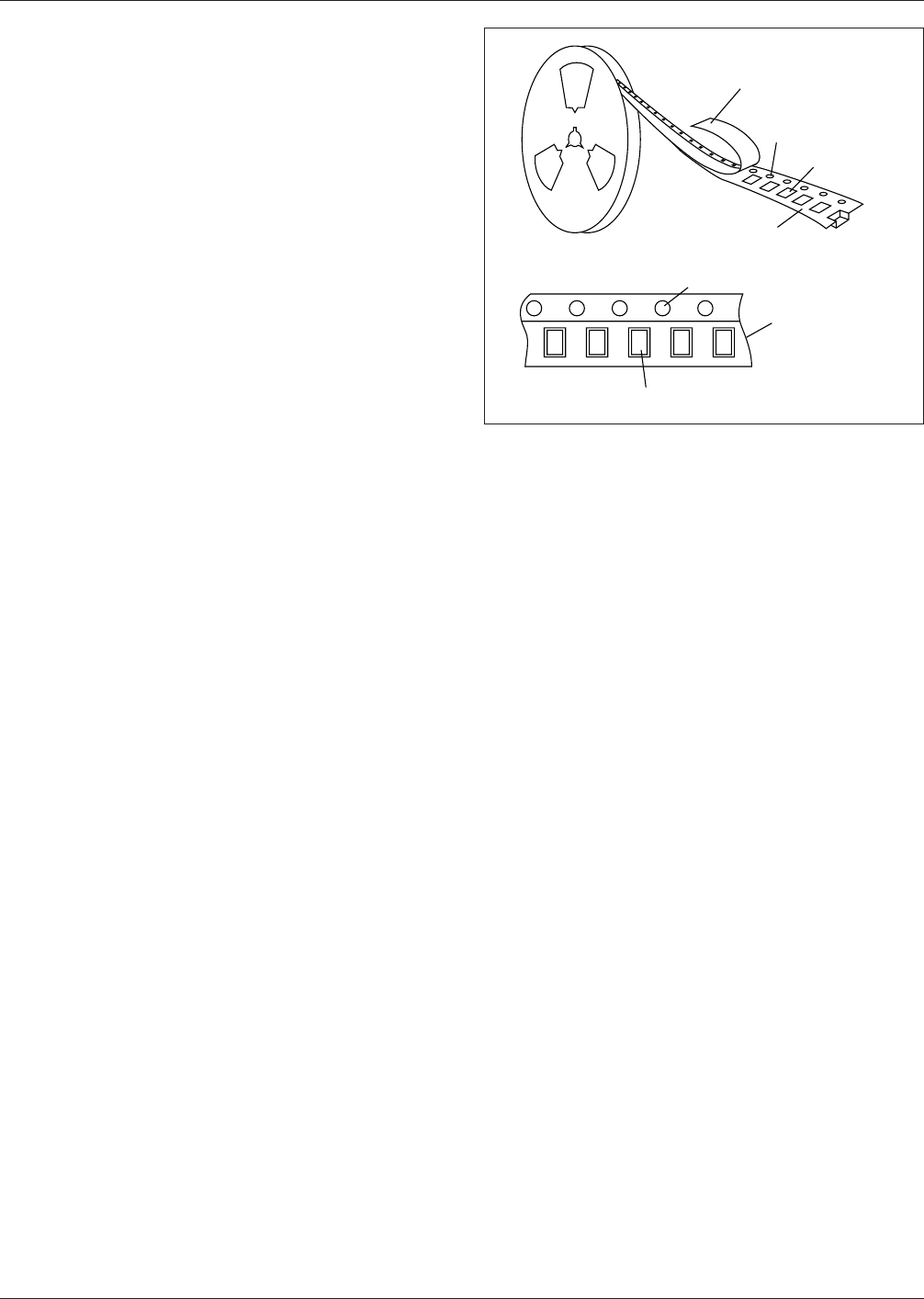
Discrete components are generally purchased in 8 mm and
12 mm wide tape and reel (see Figure 8-1). EIA-481 is the
applicable specification for tape and reel. Consult your
manufacturers guide for the packaging availability of your
component.
Parts susceptible to damage by electrostatic discharge shall
be supplied in a manner that prevents such damage. Tape
peel strength shall be 40 grams ± 30 grams. Peel from the
top for the top cover of the tape. Reel materials used in the
construction of the reel shall be easily disposable metal,
chip board, styrene plastic or equivalent. Reels shall not
cause deterioration of the components or their solderability.
Reels must be able to withstand high humidity conditions.
Parts must be capable of withstanding cleaning processes
currently used by board assembly manufacturers. This may
include as a minimum four-minute exposures to solvent
cleaning solutions at 40 °C [104 °F], plus a minimum of a
one-minute exposure to ultrasonic immersion at a fre-
quency of 40 kHz and a power of 100 watts per square
foot. Alkaline systems in use shall also not damage parts or
remove markings.
End terminations should be solder coated with a tin/lead
alloy or a lead free equivalent. The solder should contain
between 58 to 68% tin. Solder may be applied to the ter-
mination by hot dipping or by plating from solution. Plated
solder terminations should be subjected to a postplating
reflow operation to fuse the solder. The tin/lead finish
should be at least 0.0075 mm [0.0003 in] thick.
The termination shall be symmetrical, and shall not have
nodules, lumps, protrusions, etc., that compromise the sym-
metry or dimensional tolerances of the part. The end termi-
nation shall cover the ends of the components, and shall
extend out to the top and bottom of the component.
Solder finish applied over precious metal electrodes shall
have a diffusion-barrier layer between the electrode metal-
lization and the solder finish. The barrier layer should be
nickel or an equivalent diffusion barrier, and should be at
least 0.00125 mm [0.00005 in] thick.
For lead free finishes a combination of tin, silver and cop-
per is the prevalent replacement for the tin/lead finish. Sol-
derability testing should be applied per IPC-J-STD-002 to
determine attachment capability of the applicable compo-
nent type.
The following sections for each component family provide
information on basic component construction, termination
materials, marking, carrier package format and resistance
to soldering.
8.1 Chip Resistors (RESC) A variety of values exist for
resistors. This section describes the most common types.
IPC-7351-8-01
Figure 8-1 Packaging of Discrete Components
Top Cover
Tape
Sprocket
Hole
Component
Cavity
Embossed Carrier Tape
Sprocket Hole
Embossed
Carrier Tape
Component Cavity
▼
▼
▼
▼
▼
▼
▼
IPC-7351 February 2005
44
标准分享网 www.bzfxw.com 免费下载
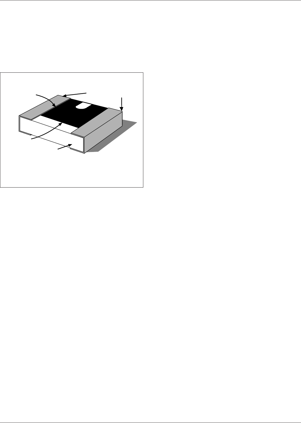
8.1.1 Basic Construction The resistive material is
applied to a ceramic substrate and terminated symmetri-
cally at both ends with a ‘‘wrap around’’ metal U-shaped
band. The resistive material is face-up, thus trimming to
close tolerances is possible. Since most equipment uses a
vacuum-type pickup head, it is important that the surface of
the resistor is made flat after trimming, otherwise vacuum
pickup might be difficult (see Figure 8-2).
8.1.2 Marking Resistors equal to or larger than 2012
[0805] are labeled. Resistors smaller than 1608 [0603] are
generally unlabeled.
8.1.3 Carrier Package Format Bulk rods, 8 mm tape/4
mm pitch is preferred for best handling. Tape and reel
specifications provide additional requirements.
8.1.4 Resistance to Soldering Parts should be capable
of withstanding five cycles through a standard reflow sys-
tem operating at 215 °C [419 °F]. Each cycle shall consist
of 60 seconds exposure at 215 °C [419 °F]. Parts must also
be capable of withstanding a minimum of 10 seconds
immersion in molten solder at 260 °C [500 °F]. See IPC/
JEDEC J-STD-020 for appropriate reflow cycles and pro-
files when using lead free solders.
8.2 Chip Capacitors (CAPC) A variety of values exist for
capacitors. This section describes the most common types.
8.2.1 Basic Construction Multilayer ceramic capacitors
use substrate materials such as alumina for hybrid circuits
and porcelainized metal. The monolithic construction used
in producing these chips results in a solid block of ceramic
with an enclosed electrode system and metallized ends for
circuit attachment. This solid block is rugged and capable
of withstanding the harsh environment and treatment asso-
ciated with manufacturing processes (see Figure 8-3). Elec-
trodes are given a common terminal by coating the chip
ends with a precious metal-glass formulation suspended in
an organic vehicle. Consecutive drying and firing elimi-
nates the organic components and affects a bond between
the ceramic dielectric and glass constituent in the termina-
tion.
8.2.2 Marking Ceramic capacitors are typically
unmarked.
8.2.3 Carrier Package Format Bulk rods, 8 mm tape/4
mm pitch is preferred for best handling. Tape and reel
specifications provide additional requirements.
8.2.4 Resistance to Soldering Parts should be capable
of withstanding five cycles through a standard reflow sys-
tem operating at 215 °C [419 °F]. Each cycle shall consist
of 60 seconds exposure at 215 °C [419 °F]. Parts must also
be capable of withstanding a minimum of 10 seconds
immersion in molten solder at 260 °C [500 °F].
Caution should be exercised when using the 4564 [1825]
capacitor mounted on organic substrates due to CTE mis-
match if the assembly sees wide temperature swings in the
assembly process or end use. See IPC/JEDEC J-STD-020
for appropriate reflow cycles and profiles when using lead
free solders.
8.3 Inductors (INDC, INDM, INDP) A variety of values
exist for inductors. This section describes the most com-
mon types.
8.3.1 Basic Construction At the time of publication,
there was no industry standard document for leadless
inductors. The dimensions were taken from manufacturer’s
catalogs, but only when at least two component vendors
manufacture the same package. However, the same induc-
tor value may not be available in the same package from
the two manufacturers (see Figure 8-4).
8.3.2 Marking Parts are available with or without
marked inductance values.
8.3.3 Carrier Package Format Bulk rods, 8 mm tape/4
mm pitch is preferred for best handling. Tape and reel
specifications provide additional requirements.
8.3.4 Resistance to Soldering Parts should be capable
of withstanding five cycles through a standard reflow sys-
tem operating at 215 °C [419 °F]. Each cycle shall consist
of 60 seconds exposure at 215 °C [419 °F]. Parts must also
be capable of withstanding a minimum of 10 seconds
immersion in molten solder at 260 °C [500 °F]. See IPC/
JEDEC J-STD-020 for appropriate reflow cycles and pro-
files when using lead free solders.
8.4 Tantalum Capacitors (CAPT) A variety of values
exist for tantalum capacitors. This section describes the
most common types.
IPC-7351-8-02
Figure 8-2 Chip Resistor Construction
Resistor
Alumina Chip
Platinum-Silver
Wrap-Around
Termination
Wire Bond Construction
Glass
Passivation
February 2005 IPC-7351
45