SOM-1655-002.pdf - 第72页
71 Tg0742-PM-SO 14. Circuit Diagrams Power Circuit Diagram (2) 14. Circuit Diagrams 0307-002-(M750WB--A3101) L1-Axis Brake OFF Multi-Layer T ray (1) Elevator and Brake OFF (Option) L2-Axis Brake OFF BPC-Axis Brake OFF Mu…
70 Tg0742-PM-SO0307-002
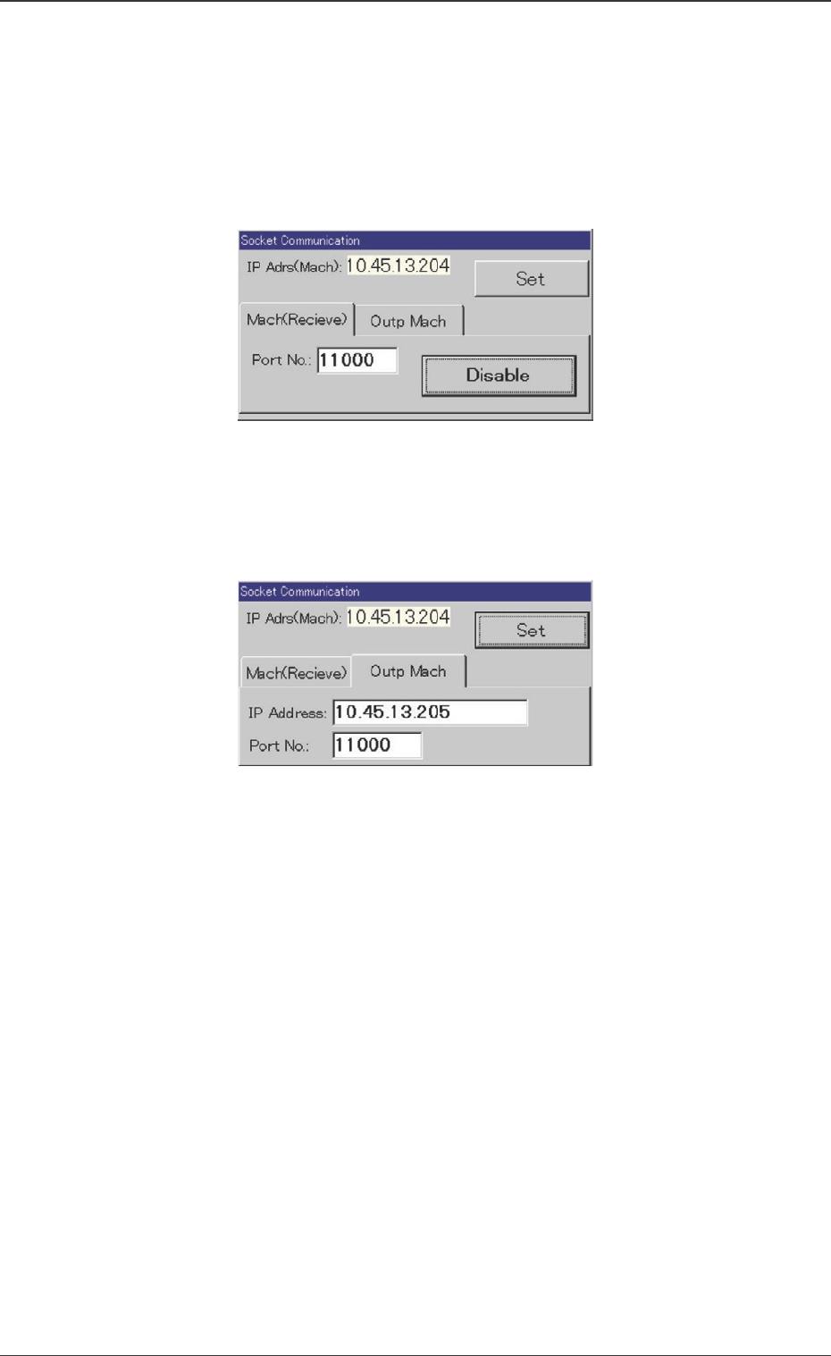
13.2 Setting Procedure for Communication with Main Machine
(2) Press the [Mach(Receive)] tab.
(3) Check the "Port No." and press the [Enable] button. Then, set
"11000" in the "Port No." data box.
(4) Press the [Disable] button.
(5) Press the [Outp Mach] tab.
(6) Set the IP address of the V. bend detection unit in the "IP
Address" data box.
(7) Set "11000" in the "Port No." data box.
(8) Press the [Set] button.
(9) Close the "Socket Communication" window.
(10) Turn off the TIM-X100 main machine and re-start.
Fig. 49
Fig. 50
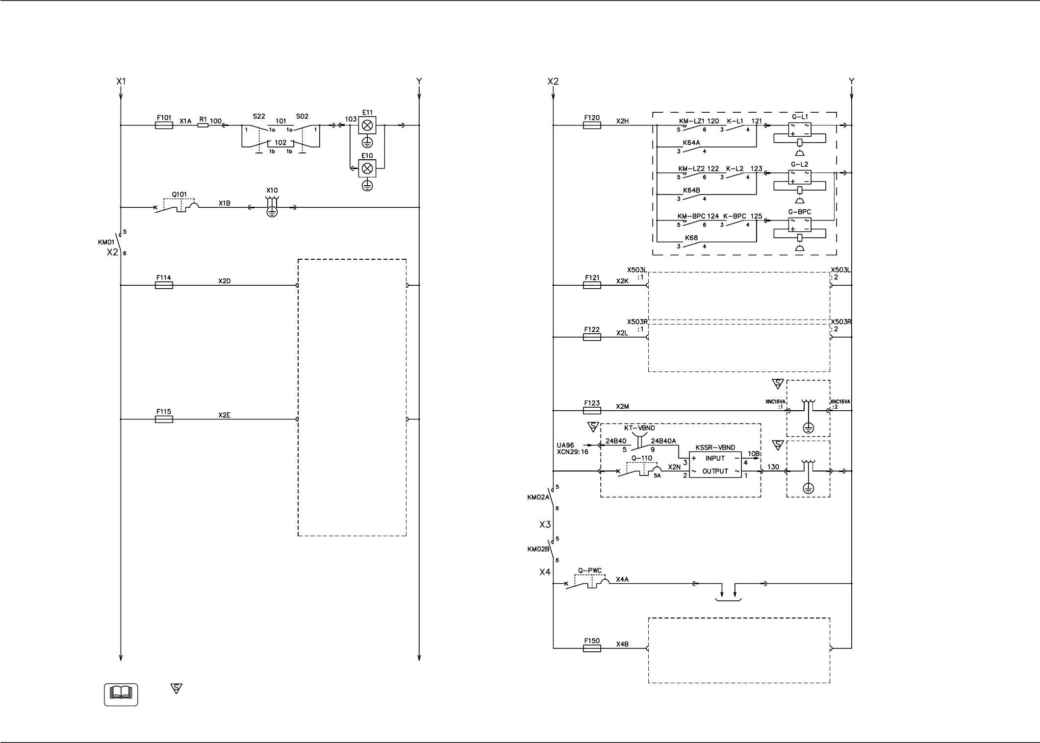
71 Tg0742-PM-SO
14. Circuit Diagrams
Power Circuit Diagram (2)
14. Circuit Diagrams
0307-002-(M750WB--A3101)
L1-Axis Brake OFF
Multi-Layer Tray (1)
Elevator and Brake OFF
(Option)
L2-Axis Brake OFF
BPC-Axis Brake OFF
Multi-Layer Tray (2)
Elevator and Brake OFF
(Option)
Power Supply for
Lead Coplanarity Detection
Power Supply for
Lead Coplanarity Detection
PWC-Axis Drive
Recycle Conveyor Motor
For Vertical Bend Detection
(Option)
Lighting for Operation
(Front Side)
Lighting for Operation
(Rear Side)
For Fan Motor
(Reserved)
For Fan Motor
(Reserved)
Console Power Supply
(Option)
Multi-Layer Tray (1)
Multi-Layer Tray (2)
(For HUB)
(For Main
Body)
To APMD-PWC
Brake
Brake
Brake
Note
The -marked area is specially specified.
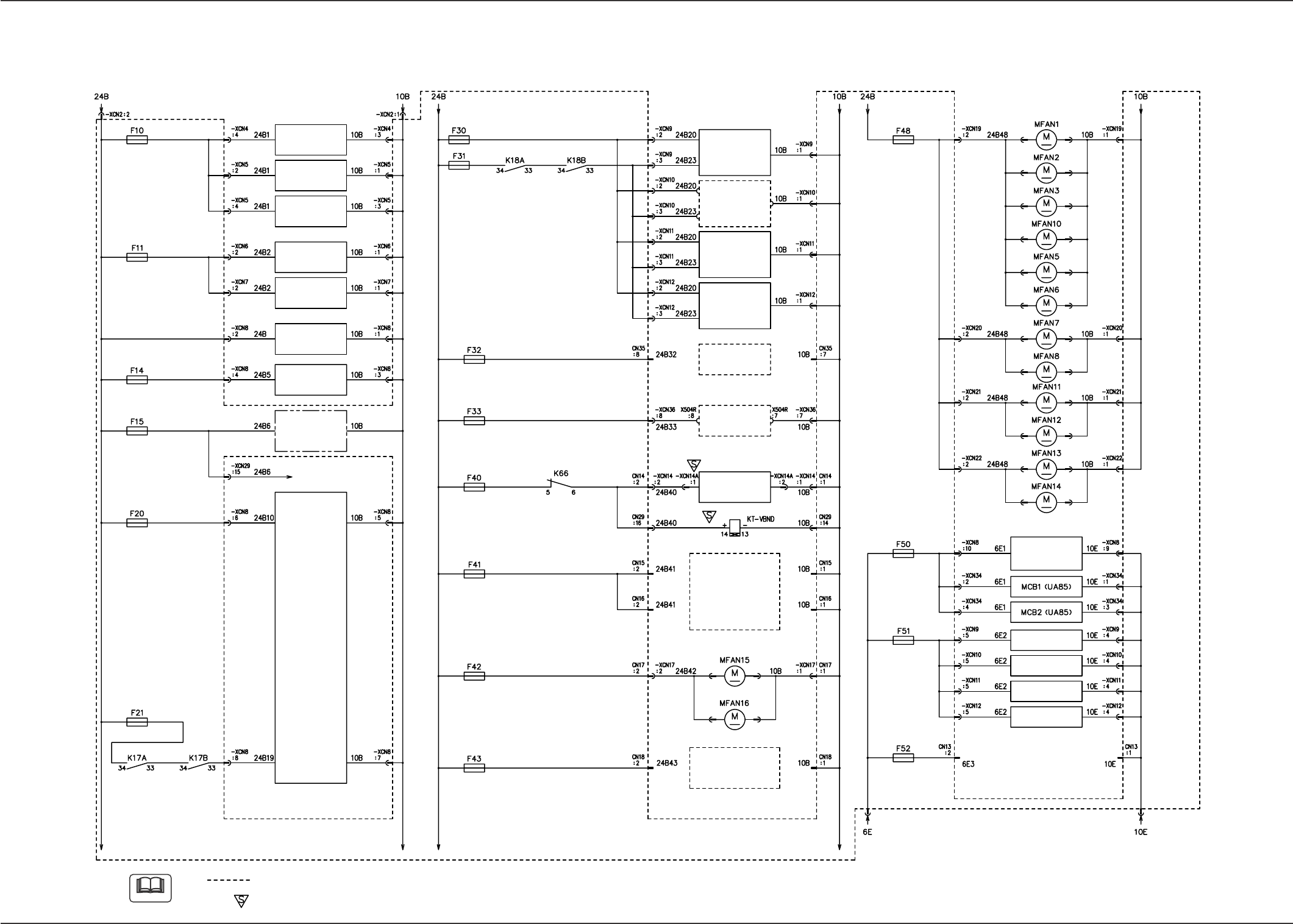
72 Tg0742-PM-SO
14. Circuit Diagrams
Power Circuit Diagram (3)
0307-002-(M750WB--A3102)
Input/Output
Machine
I/F Board (UA53)
NC1-Axis
Motor Driver
NC2-Axis
Motor Driver
Liquid Crystal
Monitor
(Rear Side)
Liquid Crystal
Monitor
(Front Side)
Lighting Control
Board
(UA75)
Motor Relay
Board
(UA93)
Relay Board
(UA96)
Brake Control Relay
Wiring Section
I/O Main Board
(UB12)
Sensor-and
Indicator-Related
Items
For Beam
Sensor 2
For Sensor on
Frame Top
For Panel 1
For Panel 2
For Cover Top
For Electromagnetic
Valve
DC Load Supply 1 DC Load Supply 2
Feeder Power
Supply 1
Feeder Power
Supply 2
Feeder Base #1
Feeder Base #2
(Option)
Feeder Base #3
Feeder Base #4
(Multi-Layer Tray 1 (Option))
(Multi-Layer Tray 2 (Option))
(BCR Option)
(Option)
Sensor Head for
Chip Inspector
(Vertical Bend Detection (Option))
Right Side Fun Motor
Left Side Fun Motor
Frame Lower
R Side 1
Fan Motor
Frame Lower
R Side 2
Fan Motor
Frame Lower
R Side 3
Fan Motor
Frame Lower
Front Side
Fan Motor
Frame Lower
L Side 1
Fan Motor
Frame Lower
L Side 3
Fan Motor
Frame Lower
L Side 2
Fan Motor
Frame Lower
L Side 4
Fan Motor
Frame Top
Exhaust
Fan Motor 1
Frame Top
Exhaust
Fan Motor 2
Frame Top
Exhaust
Fan Motor 3
Frame Top
Exhaust
Fan Motor 4
I/O Main Board
(UB12)
Feeder Base #1
Feeder Base #2
Feeder Base #3
Feeder Base #4
Note (a)
Note
(a) The diagram within broken lines shows one within relay PCB (UA96).
(b) The -marked area is specially specified.