MIL- STD-883F 2004 TEST METHOD STANDARD MICROCIRCUITS.pdf - 第138页
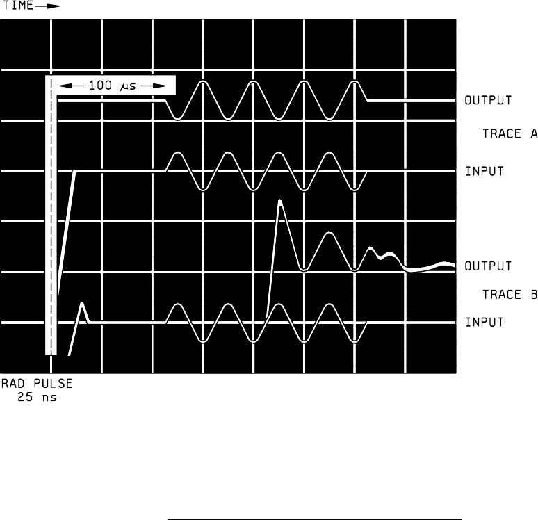
MIL-STD-883F METHOD 1020.1 15 November 1991 10 FIGURE 1020-2. Linear devic e latc hup sc reen tes t photogr aph (50 µ s/di v) .
MIL-STD-883F
METHOD 1020.1
15 November 1991
9
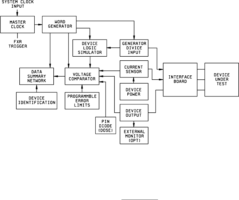
FIGURE 1020-1. Latchup system
.
MIL-STD-883F
METHOD 1020.1
15 November 1991
10
FIGURE 1020-2. Linear device latchup screen test photograph (50 µs/div)
.

MIL-STD-883F
METHOD 1021.2
15 November 1991
1
METHOD 1021.2
DOSE RATE UPSET TESTING OF DIGITAL MICROCIRCUITS
1. PURPOSE
. This test procedure defines the requirements for testing the response of packaged digital integrated
circuits to pulsed ionizing radiation. A flash x-ray or linear accelerator is used as a source of pulses of ionizing radiation.
The response may include transient output signals, changes in the state of internal storage elements, and transient current
surges at inputs, outputs, and power supply connections. The dose rate at which logic or change-of-state errors first occur
is of particular interest in many applications.
1.1 Definitions
. Definitions of terms used in this procedure are given below:
a. Dose rate threshold for upset. The dose rate which causes either:
(1) A transient output upset for which the change in output voltage of an operating digital integrated circuit goes
either above or below (as appropriate) specified logic levels (see 3.2 on transient voltage criteria), and the
circuit spontaneously recovers to its preirradiation condition after the radiation pulse subsides, or
(2) A stored data or logic state upset for which there is a change in the state of one or more internal memory or
logic elements that does not
recover spontaneously after the radiation pulse. However, the circuit can be
restored to its preirradiation condition by applying the same sequence of logic signals to its inputs that were
previously used to establish the preirradiation condition, or
(3) A dynamic upset which results in a change in the expected output or stored test pattern of a device that is
functionally operating during the time it is irradiated. The upset response may depend on the precise time
relationship between the radiation pulse and the operating cycle of the device. For operations requiring
many clock signals, it may be necessary to use a wide radiation pulse.
b. Dose rate. Energy absorbed per unit time per unit mass by a given material from the radiation field to which it is
exposed.
c. Combinational logic circuit. A digital logic circuit with the property that its output state is solely determined by the
logic signals at its inputs. Combinational logic circuits contain no internal storage elements. Examples of
combinational circuits include gates, multiplexers, and decoders.
d. Sequential logic circuit. A digital logic circuit with the property that its output state at a given time depends on the
sequence and time relationship of logic signals that were previously applied to its inputs. Sequential logic circuits
contain internal storage elements. Examples of sequential logic circuits include memories, shift registers,
counters, and flip-flops.
e. State vector. A state vector completely specifies the logic condition of all elements within a logic circuit. For
combinational circuits the state vector includes the logic signals that are applied to all inputs; for sequential
circuits the state vector must also include the sequence and time relationship of all input signals (this may include
many clock cycles).