MIL- STD-883F 2004 TEST METHOD STANDARD MICROCIRCUITS.pdf - 第422页
MIL-STD-883F METHOD 2032.2 18 June 2004 16 Class H Cla ss K 3.1.3 Gl assi vation defec ts , "high magnif icat ion" . No device s hall be ac ceptabl e that exhibit s: NOTE: Cri teria of 3.1.3 c an be excluded wh…
MIL-STD-883F
METHOD 2032.2
18 June 2004
15
Class H Class K
3.1.2 Passivation defects "high magnification"
.
No element shall be acceptable that
exhibits:
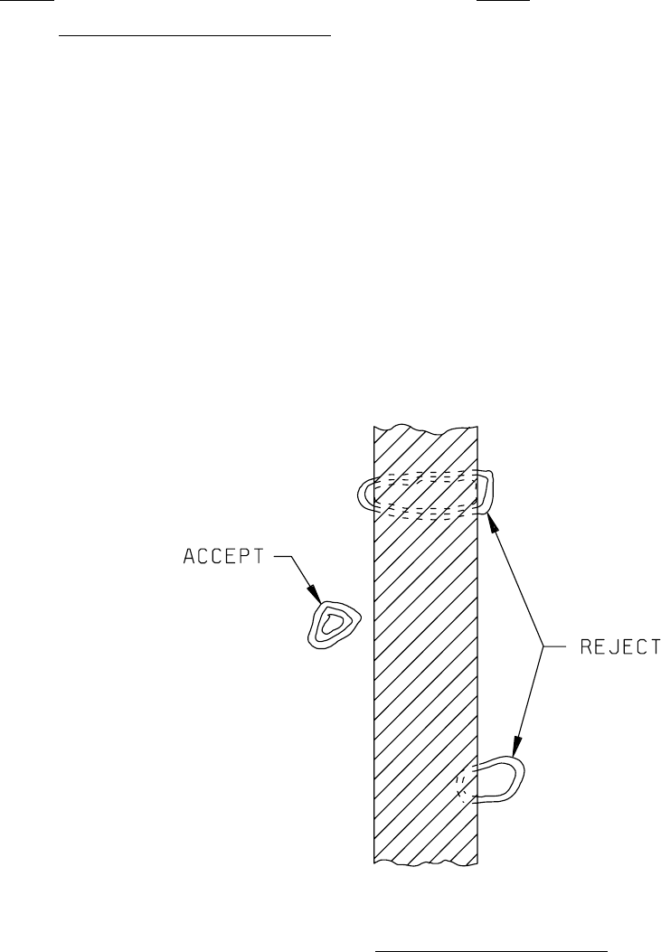
a. Either multiple lines (color fringing) or a a. Same as class H.
complete absence of passivation visible at
the edge and continuing under the
metallization (see figure 2032-8Ah).
A passivation defect that exhibits a line
of separation from the metallization is
acceptable.
NOTE: These criteria apply to conductive
substrate elements only.
NOTE: Double or triple lines at the edge
of the passivation defect indicate it can
have sufficient depth to penetrate down to
the bare substrate.
FIGURE 2032-8Ah. Class H passivation defect criteria
.
MIL-STD-883F
METHOD 2032.2
18 June 2004
16
Class H Class K
3.1.3 Glassivation defects, "high magnification"
.
No device shall be acceptable that exhibits:
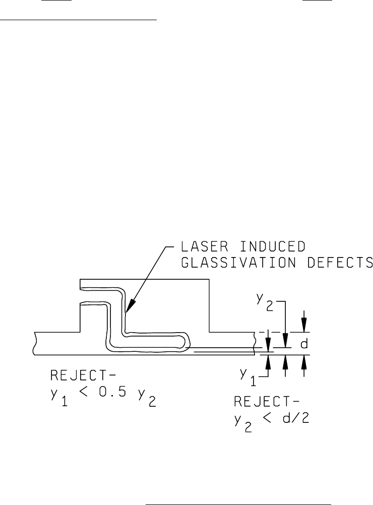
NOTE: Criteria of 3.1.3 can be excluded when the
defects are due to laser trimming. In this case,
the defects outside the kerf due to laser
trimming shall not be more than one half the
remaining resistor width and shall leave a
primary resistor path free of glassivation
defects, equal to or greater than 50 percent
of the narrowest resistor width,
(see figure 2032-9h).
FIGURE 2032-9h. Class H laser trimmed glassivation defect criteria
.
a. Glass crazing or damage that prohibits the a. Same as class H.
detection of visual criteria contained herein.

MIL-STD-883F
METHOD 2032.2
18 June 2004
17
Class H Class K
3.1.3 b. Any lifting or peeling of the glassivation. 3.1.3 b. Same as class H.
NOTE: Lifting or peeling of the
glassivation is acceptable when it does not
extend more than 1.0 mil from the designed
periphery of the glassivation, provided that
the only exposure of metallization is of
adjacent bonding pads or of metallization
leading from those pads.
c. A void in the glassivation that exposes c. Same as class H.
two or more adjacent operating
metallization paths, excluding bonding
pad cutouts, unless by design.
d. Unglassivated nonactive circuit areas greater d. Same as class H.
than 5.0 mils in any dimension, unless by
design.
e. Unglassivated areas at the edge of a bonding e. Same as class H.
pad exposing the conductive substrate.
f. Glassivation covering more than 25 percent f. Same as class H.
of a bonding pad area.
g. Crazing in glassivation over a resistor. g. Same as class H.
h. Misalignment of the glassivation that h. Same as class H.
results in incomplete coverage of a
resistor, unless by design.
i. Glassivation scratches or voids that i. Same as class H.
expose any portion of a resistor or
fusible link except for polycrystalline
silicon links where the glassivation is
opened by design.
j. Scratches in the glassivation that disturb j. Same as class H.
metallization and bridge metallization
paths.
k. Cracks (not crazing) in the glassivation k. Same as class H.
that form a closed loop over adjacent
metallization paths.