MIL- STD-883F 2004 TEST METHOD STANDARD MICROCIRCUITS.pdf - 第414页
MIL-STD-883F METHOD 2032.2 18 June 2004 8 3.1.1 .2 Metalliz ation vo ids . a. Vo id(s) in the m etalliza tion, ex cludin g a. Same a s Class H bonding pads , that leaves l ess t han 50 per cent of the original m etalliza…
MIL-STD-883F
METHOD 2032.2
18 June 2004
7
Class H
Class K
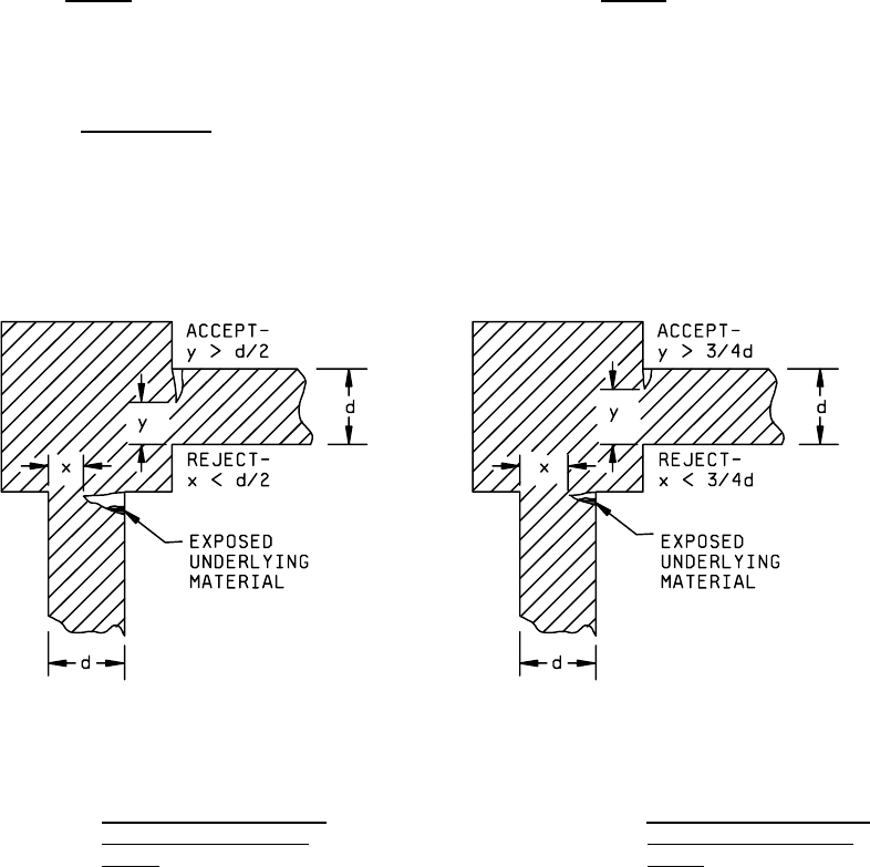
3.1.1.1 b. Scratch in the bonding pad area 3.1.1.1 b. Less than 75 percent (see
that both exposes underlying material and figure 2032-2k).
reduces the metallization path width,
where it enters the bonding pad, and leaves
less than 50 percent
of its original
metallization width. If two or more
metallization paths enter a bonding pad,
each shall be considered separately
(see figure 2032-2h).
FIGURE 2032-2h. Class H metallization width
FIGURE 2032-2k. Class K metallization width
reduction at bonding pad
reduction at bonding pad
criteria
. criteria.
3.1.1.1 c. Scratch that completely crosses a c. Same as class H.
Metallization path and damages the
surface of the surrounding
passivation, glassivation, or substrate on
either side.
d. Scratches or probe marks in the d. Same as class H.
bonding pad area that expose
underlying material over greater
than 25 percent of the original
unglassivated metallization area.
e .For capacitors only, a scratch in the e. Same as class H.
metallization, other than in the bonding
pad area, that exposes the dielectric
material.
MIL-STD-883F
METHOD 2032.2
18 June 2004
8
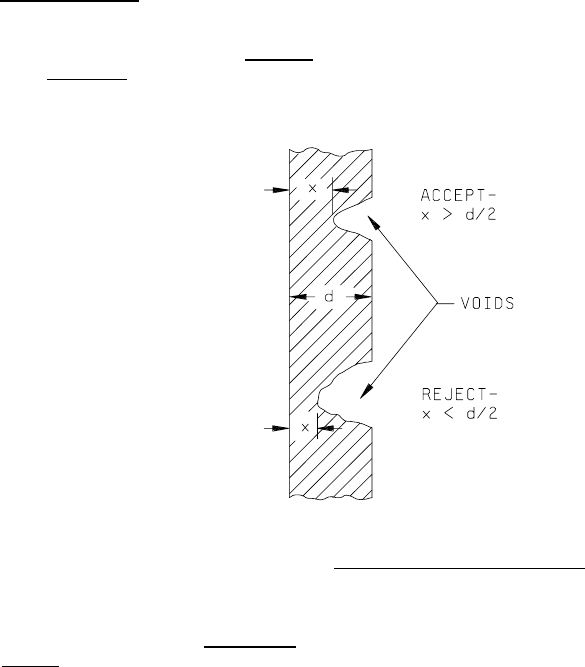
3.1.1.2 Metallization voids
.
a. Void(s) in the metallization, excluding a. Same as Class H
bonding pads, that leaves less than
50 percent
of the original metallization
width undisturbed (see figure 2032-3h).
FIGURE 2032-3h. Class H metallization void criteria
.
b. Void(s) in the bonding pad area that reduces b. Less than 75 percent
the metallization path width, where it
enters the bonding pad, to less than 50
percent
of its original metallization width.
If two or more metallization paths enter a
bonding pad, each shall be considered
separately.
NOTE: Figures 2032-2h and 2032-2k
illustrate metallization width reduction
at bonding pad criteria for scratches.
Void criteria are similar.
MIL-STD-883F
METHOD 2032.2
18 June 2004
9
Class H Class K
3.1.1.2 c. Void(s) in the bonding pad area that 3.1.1.2 c. Same as class H.
expose underlying material over greater
than 25 percent of the original
unglassivated metallization area.
NOTE: For RF/microwave elements on nonconductive
substrates, a void created in the bonding
pad area as a result of wire bond removal for
performance optimization or tuning, is not
rejectable provided that the void remains
entirely visible.
d. For capacitors only, void(s) in d. Same as class H.
metallization, other than in the bonding
pad area, that reduces the metallization
to an extent greater than an area
equivalent to 25 percent of the
capacitor metallization.
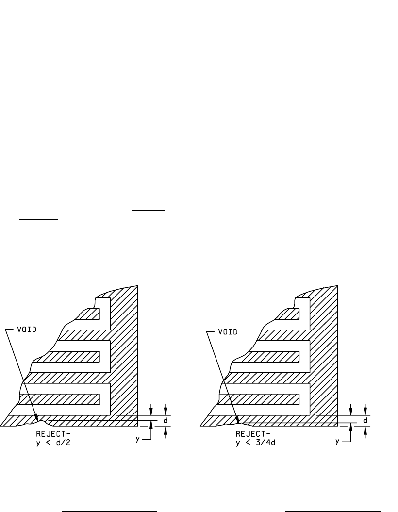
e. For interdigitated capacitors only, void(s) e. Less than 75 percent (see
in the metallization that leaves less than
figure 2032-4k).
50 percent
of the original metallization
width undisturbed (see figure 2032-4h).
FIGURE 2032-4h. Class H interdigitated capacitor
FIGURE 2032-4k. Class K interdigitated capacitor
metallization void criterion
. metallization void criterion.