MIL- STD-883F 2004 TEST METHOD STANDARD MICROCIRCUITS.pdf - 第525页
MIL-STD-883F METHOD 3017 29 May 1987 3 h. C L (min). i. L L (max ). j. L L (min). k. R M (max ). l. R M (min). m. R L (max ). n. R L (min). o. Pac kage pins to be tes ted. p. Pac kage ground c onfigur ation.

MIL-STD-883F
METHOD 3017
29 May 1987
2
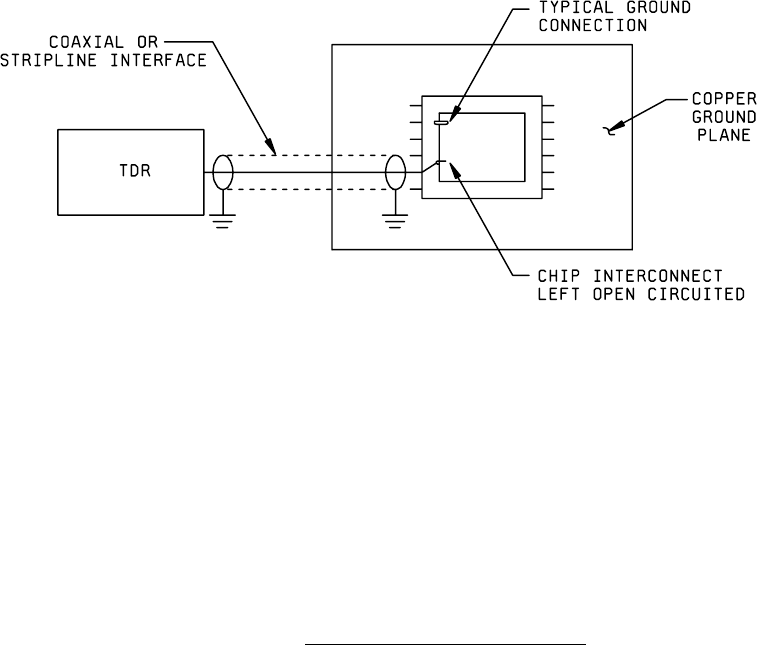
3.2 Test procedure for package transmission characteristics. Using a section of coaxial cable of known, calibrated
characteristic impedance (Z
Ref
) as a reference measure the minimum (Z
Min
) maximum (Z
Max
) and average (Z
o
) values of
reflection coefficient (
ρ) for the section of line on the TDR display that has been carefully determined to be the package pin
(locate using zero-length short circuits).
3.2.1 Characteristic impedance
. Calculate characteristic impedance (Z
o
) for each of the cases from the formula:
0Ref
Z
=
Z
x
(1+ )
(1- )
ρ
ρ
3.2.2 Delay time measurement
. From the TDR display of 3.2.1 measure the time difference in picoseconds from the point
identified as the start of the exterior package pin (t
1
) to the chip interface point (t
2
) (t = t
1
-t
2
)
Form the package design drawings, determine the physical length of the package run (L)
Time delay
t
=
t
L
pd
∆
3.2.3 Load capacitance calculation
.
Load capacitance
C
=
t
Z
L
pd
o
3.2.4 Load inductance calculation
.
Load inductance (series) =
(
t
)
C
pd
2
L
3.3. Series resistance measurement
.
Using the test setups of figure 3017-2, separately measure the dc resistance of the chip-to-package interface media (R
M
)
and the package lead (R
L
).
4. SUMMARY
. The following details, when applicable, shall be specified in the applicable acquisition document:
a. Z
Max
.
b. Z
Min
.
c. Z
o
(max).
d. Z
o
(min).
e. t
pd
(max).
f. t
pd
(min).
g. C
L
(max).
*
MIL-STD-883F
METHOD 3017
29 May 1987
3
h. C
L
(min).
i. L
L
(max).
j. L
L
(min).
k. R
M
(max).
l. R
M
(min).
m. R
L
(max).
n. R
L
(min).
o. Package pins to be tested.
p. Package ground configuration.
MIL-STD-883F
METHOD 3017
29 May 1987
4
FIGURE 3017-1. Time domain reflectometer test setup
.