MIL- STD-883F 2004 TEST METHOD STANDARD MICROCIRCUITS.pdf - 第234页
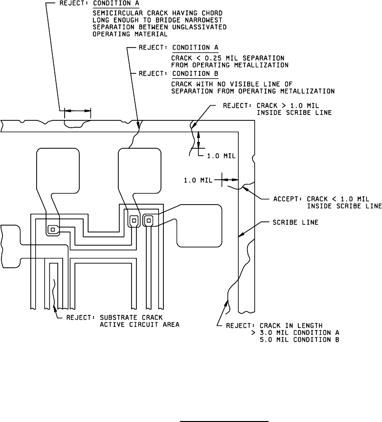
MIL-STD-883F METHOD 2010.11 18 June 2004 24 FIGURE 2010-22 Sc ribi ng and die defec ts .

MIL-STD-883F
METHOD 2010.11
18 June 2004
23
Condition A Condition B
Class level S Class level B
3.1.3 Scribing and die defects
. No device shall be acceptable that exhibits:
a. Less than 0.25 mil of passivation visible a. No line of separation between operating
between operating metallization or bond metallization or bond periphery and bare
periphery and bare semiconductor material semiconductor material (see figure 2010-22).
(see figure 2010-22).
NOTE: For GaAs devices only, less than 0.1 mil of substrate visible between operating metallization or bond periphery
and edge of the die.
NOTE: Criteria can be excluded for beam leads and peripheral metallization including bonding pads where the
metallization is at the same potential as the substrate.
NOTE: Does not apply to SOS devices.
b. A chipout or crack in the active circuit area (see figures 2010-22 and 2010-38). In addition for GaAs a chipout into
or underneath the functional metallization, e.g., bond pads, capacitors, peripheral metallization, etc., but excluding
test structures of the device.
NOTE: Criteria can be excluded for peripheral metallization that is at the same potential as the substrate. At least 50
percent undisturbed metallization width shall remain at the chipout.
c. A crack that exceeds 3.0 mils in length, or c. A crack that exceed 5.0 mils in length, or
comes closer than 0.25 mils to any operating that does not exhibit a line of separation to
metallization (except for substrate potential any operating metallization (except for
peripheral metal) or functional circuit element substrate potential peripheral metal) or
(see figure 2010-22). function circuit element (see figure 2010-22).
d. For condition A only. Semicircular crack(s) d. No condition B.
terminating at the die edge, whose chord is long
enough to bridge the narrowest spacing between
unglassivated operating material (e.g.,
metallization, bare semiconductor material,
mounting material, bonding wire, etc.) (see figure
2010-22).
e. Exposed semiconductor material extending over the passivation edge at the point of the beam lead exit from the
die (applicable to beam lead structures only) (see figure 2010-38).
f. Die having attached portions of the active circuit area of another die.
g. A crack that exceeds 1.0 mil in length inside the scribe line (or semiconductor material edge for beam lead
devices) that points toward operating metallization or functional circuit elements (see figure 2010-22).
h. A crack that comes closer than 0.5 mil to operating beam lead metallization (see figure 2010-38).
NOTE: Criteria of 3.1.3c and h can be excluded for beam lead devices where the chipout or crack does not extend
into the semiconductor material.
NOTE: Criteria of 3.1.3e and h do not apply to GaAs devices.
MIL-STD-883F
METHOD 2010.11
18 June 2004
24
FIGURE 2010-22 Scribing and die defects.
MIL-STD-883F
METHOD 2010.11
18 June 2004
25
Condition A Condition B
Class level S Class level B
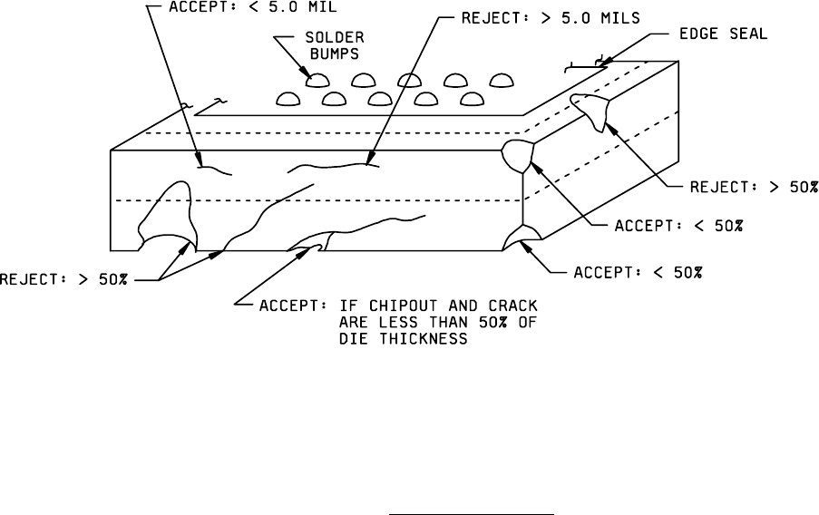
i. For flip chip, cracks, or chipouts in the substrate material that extends beyond 50 percent of substrate thickness
or a crack greater than 5.0 mils in length in the substrate material (see figure 2010-23).
FIGURE 2010-23. Scribing and die defects
.
j. Any blistering, peeling, delamination, corrosion, or other gross defects in glassivation, metal, interlevel dielectrics
or other layers.