MIL- STD-883F 2004 TEST METHOD STANDARD MICROCIRCUITS.pdf - 第238页
MIL-STD-883F METHOD 2010.11 18 June 2004 28 Condition A Conditi on B Class le vel S Class lev el B c . A diff used area whi ch over laps di elect ric isol ation mater ial and does not exhibit a line of s eparat ion to an…
MIL-STD-883F
METHOD 2010.11
18 June 2004
27
Condition A Condition B
Class level S Class level B
h. Scratch(es) in the glassivation that disturbs metal and bridges metallization paths.
i. Crack(s) (not crazing) in the glassivation that forms a closed loop over adjacent metallization paths.
j. Glassivation void(s) that exposes any portion of a thin film resistor or fusible link except where the glassivation is
opened by design.
k. For GaAs devices, voids in the glassivation that extends over the gate channel of the FET.
l. For GaAs devices, scratches in the glassivation over the gate channel of the FET.
m. For GaAs devices, scratches in the glassivation over the gate insertion of the FET.
n. For GaAs devices, cracks in the glassivation which are more than 1.0 mil inside the scribe line, or are more than
50 percent of the distance between the scribe line and any functional or active element (e.g., capacitor, resistor,
FET) and which point toward any functional or active element unless the crack terminates at a device feature
(e.g., transmission line or dc line).
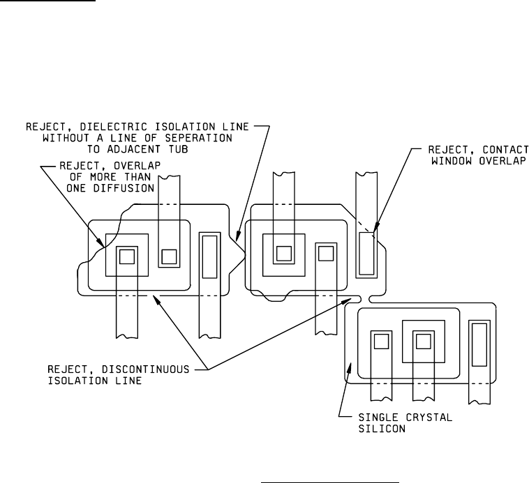
3.1.5 Dielectric isolation
. No device shall be acceptable that exhibits:
a. A discontinuous isolation line (typically a black line) around each diffusion tub containing functional circuit
elements (see figure 2010-25).
b. Absence of a continuous isolation line between any adjacent tubs, containing functional circuit elements (see
figure 2010-25).
FIGURE 2010-25. Dielectric isolation defects
.
MIL-STD-883F
METHOD 2010.11
18 June 2004
28
Condition A Condition B
Class level S Class level B
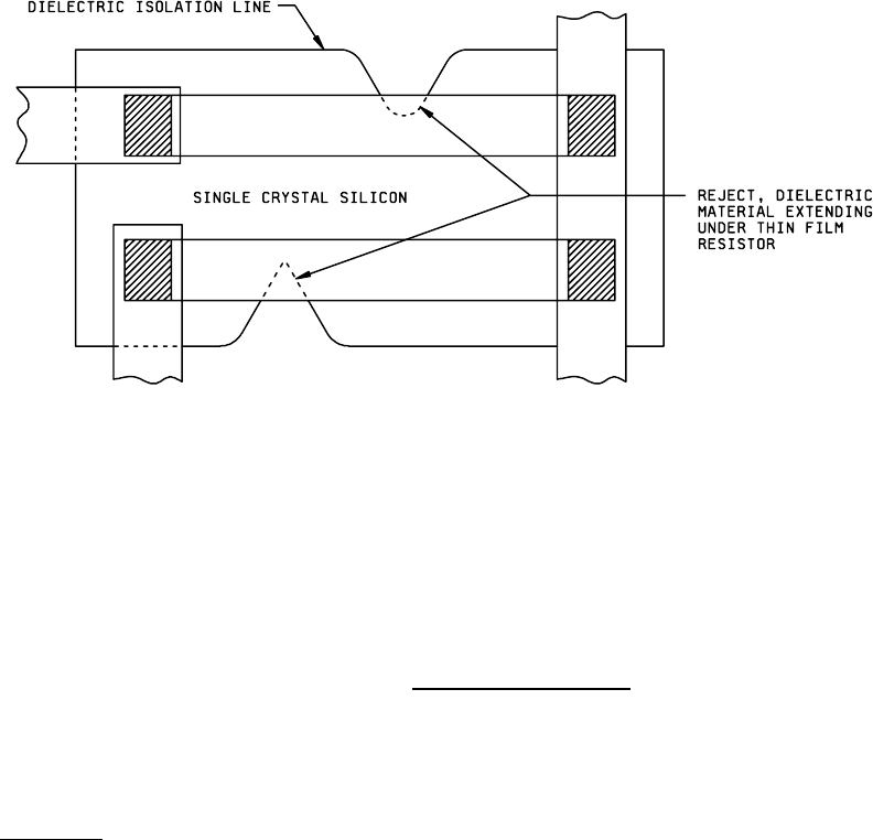
c. A diffused area which overlaps dielectric isolation material and does not exhibit a line of separation to an adjacent
tub, or an overlap of more than one diffusion area into the dielectric isolation material (see figure 2010-25).
FIGURE 2010-26. Dielectric isolation defects
.
d. A contact window that touches or overlaps dielectric material, except by design.
NOTE: Metallization scratch and void defects over a dielectric isolation step shall be rejected in accordance with
criteria contained in 3.1.1.1d and 3.1.1.2b.
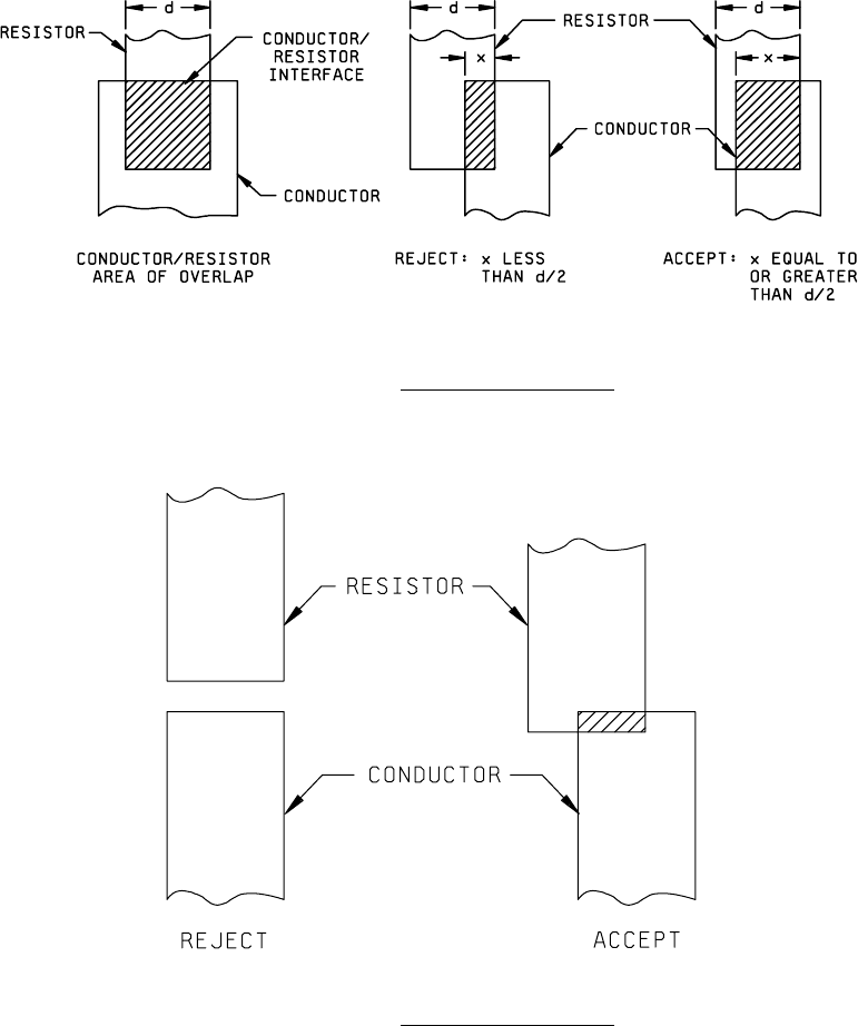
3.1.6 Film resistor
. Rejection shall be based on defects found within the actively used portions of the film resistor.
Metallization defect criteria of 3.1.1 shall apply as applicable. No device shall be acceptable that exhibits:
MIL-STD-883F
METHOD 2010.11
18 June 2004
29
Condition A Condition B
Class level S Class level B
a. Any misalignment between the conductor/resistor in which the actual width X of the overlap is less than 50
percent of the original resistor width.
FIGURE 2010-27. Film resistor contact area
.
b. No visible line of contact overlap between the metallization and film resistor (see figure 2010-28).
FIGURE 2010-28. Film resistor contact area
.