MIL- STD-883F 2004 TEST METHOD STANDARD MICROCIRCUITS.pdf - 第317页
MIL-STD-883F METHOD 2018.4 18 June 2004 5 3.1.2 Sampl ing Destr ucti ve Physic al Analys is ( DPA) eval uation . Fi nished pr oduct , wafers , or die may be subjec ted to t he test condit ions and c rit eria def ined wit…
MIL-STD-883F
METHOD 2018.4
18 June 2004
4
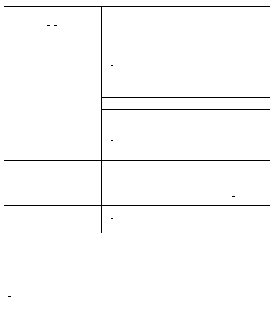
TABLE I. Wafer sampling procedures for various metallization chamber configurations.
Metallization chamber
configuration
1
/ 2/
Number of
wafer lots
in chamber
3
/
Required number of
samples per wafer lot
Sampling plans
per wafer lot
Evaporation Sputtering
Projected plane view of the
Wafer-holder is a circle.
Wafer-holder is stationary
or "wobbulates"
1
4
/
5 2 Four from near the
periphery of the wafer-
holder and 90° apart.
One from the center of
holder. See figure 4.
2 3, 4, or 5 2 See figure 4.
3 3 or 4 2 See figure 4.
4 3 2 See figure 4.
Wafer-holder is symmetrical
(i.e., circular, square, etc.).
Deposition source(s) is above or below
the wafer-holder. Wafer-holder
rotates about its center during
deposition.
1, 2, 3,
or 4
4
/
2 2 For each wafer lot, one
from the periphery of the
wafer-holder, and one
from close proximity to
the center of rotation.
See figure 4. 5
/
Planetary system. One or more
symmetrical wafer-holders (planets)
rotate about their own axes while
simultaneously revolving about the
center of the chamber. Deposition
source(s) is above or below
the wafer-holders.
1, 2, 3,
or 4 per
planet
4
/
2 2 For each wafer lot, one
from near the periphery
of a planet and one from
near the center of the
same planet. See
figure 4. 6
/
Continuous feed. Wafers are
continuously inserted into deposition
chamber through a separate pump down
of an airlock (25 wafer nominal load)
1
1
/
2 2 Two randomly selected
wafers from each wafer
lot.
1
/ In this case, a wafer lot shall be defined as a batch of wafers which have received together those common processes
which determine the slope and thickness of the passivation steps on these wafers.
2
/ If a wafer-holder has only one circular row, or if only one row is used on a multi-rowed wafer-holder; the total number
of specified sample wafers shall be taken from that row.
3
/ If there is more than one wafer lot in a metallization chamber, each wafer lot shall be grouped approximately in a
separate sector within the wafer-holder. A sector is an area of the circular wafer-holder bounded by two radii and the
subtended arc; quadrants and semicircles are used as examples on figure 4.
4
/ If the wafer lot size exceeds the loading capacity of the metallization system each processed sub-lot will be sampled
as if it was a unique lot.
5
/ When evaluation data shows that there is no relationship between SEM results and the physical location of the
wafers during the metallization process. It shall be permissible to substitute two randomly selected wafers from each
wafer lot. This analysis shall be repeated after each major equipment repair.
6
/ Sample wafers need be selected from only one planet if all wafer lots contained in the chamber are included in that
planet. Otherwise, sample wafers of the wafer lot(s) not included in that planet, shall be selected from another
planet(s).

MIL-STD-883F
METHOD 2018.4
18 June 2004
5
3.1.2 Sampling Destructive Physical Analysis (DPA) evaluation. Finished product, wafers, or die may be subjected to the
test conditions and criteria defined within this test method for the purpose of a DPA evaluation.
3.2 Lot control during SEM examination
. After dice selection for SEM examination, the manufacturer may elect either of
two options:
3.2.1 Option 1
. The manufacturer may continue normal processing of the lot with the risk of later recall and rejection of
product if SEM inspection, when performed, shows defective metallization. If this option is elected, positive control and
recall of processed material shall be demonstrated by the manufacturer by having adequate traceability documentation.
3.2.2 Option 2
. Prior to any further processing, the manufacturer may store the dice or wafers in a suitable environment
until SEM examination has been completed and approval for further processing has been granted.
3.3 Specimen preparation
. When applicable, glassivation shall be removed from the dice using an etching process that
does not damage the underlying metallization to be inspected (e.g., chemical or plasma etch). Specimens shall be mounted
for examination in a manner appropriate to the apparatus used for examination. Suitable caution shall be exercised so as
not to obscure features to be examined.
Specimens may be examined without any surface coating if adequate resolution and signal-to-noise levels are obtained. If
the specimens need to be coated, they shall be coated with no more than 100Å of a thin vapor-deposited or sputtered film of
a suitable conductive material (e.g., Au). The coating deposition process shall be controlled such that no artifacts are
introduced by the coating.
3.4 Specimen examination, general requirements
. The general requirements for SEM examination of general
metallization and passivation step coverage are specified below in terms of directional edge, magnification, viewing angle,
and viewing direction.
3.4.1 Directional edge
. All four directional edges of every type of passivation step (contact window or other type of
passivation step) shall be examined on each specimen (see table II).
3.4.2 Magnification
. The magnification used for examination of general metallization and passivation steps shall be within
the range defined by table II.
3.4.3 Viewing angle
. Specimens shall be viewed at whatever angle is appropriate to accurately assess the quality of the
metallization. Contact windows, metal thickness, lack of adhesion, and etching defects are typically viewed at the angles of
0° to 85° (see figure 2018-3).
3.4.4 Viewing direction
. Specimens shall be viewed in an appropriate direction to accurately assess the quality of the
metallization. This inspection shall include examination of metallization at the edges of contact windows and other types of
passivation steps (see 3.4) in any direction that provides clear views of each edge and that best displays any defects at the
passivation step. This may mean that the viewing angle is perpendicular to an edge, or in parallel with an edge, or at some
oblique angle to an edge, whichever best resolves any question of defects at the passivation step (see figure 2018-5).
3.5 Specimen examination detail requirements
. Examination shall be as specified herein and summarized in table II. The
specimen examination shall be documented in accordance with 3.8.
3.5.1 General metallization
. At low magnification, inspect at least 25 percent or 10,000 square mils, whichever is less, of
the general metallization on each die for defects such as lifting, peeling, blistering, and voiding. Inspection shall be
performed for each layer of each level of metallization.
3.5.1.1 Multi-layer and multi-level metal interconnection systems
. Each layer of each metallization level that is deposited
shall be examined. The current- carrying layer(s) shall be examined with the SEM after removal of the glassivation layer (if
applicable) with a suitable etchant (see 3.3).
MIL-STD-883F
METHOD 2018.4
18 June 2004
6
3.5.1.2 Barrier/adhesion layers. The examination of barrier/adhesion layers designed to conduct less than 10% of the
total current is not required as this is considered a non-conduction layer.
3.5.1.2.1 Barrier/adhesion layer as a conductor
. The barrier/adhesion layer shall be considered as a conductor
(considering the layer thickness and relative conductivity) provided that the following conditions are satisfied: At least ten
percent of the current is designed to be carried by this layer; and this layer is used in the current density calculations. When
this occurs the barrier/ adhesion layer and/or the principal conducting layer shall satisfy all of the step coverage
requirements collectively as baselined by the manufacturer. Specimen examination shall be in accordance with 3.5 and the
accept/reject criteria as defined in 3.7.1. The barrier/adhesion layer(s) shall be examined using either the SEM or optical
microscope. The following methods may be used to examine these barrier/adhesion layers:
3.5.1.2.1.1 The Etchback procedure
. This involves the stripping of each successive unique layer of metal by selective
etching, with suitable etchants, layer by layer, to enable the examination of each layer. Typically, each successive layer of
metal will be stripped in sequence to expose the next underlying layer for examination. Successive layer removal on a
single die area may be impractical. In this case the wafer area or additional die (dice) immediately adjacent on the slice to
the original die area shall be stripped to meet the requirement that all unique layers shall be exposed and examined.
3.5.1.2.1.2 In-line procedure
. The wafer(s) shall be inspected for the defined accept/reject criteria immediately after
being processed through each unique deposition and corresponding etching operation.
3.5.2 Passivation steps
. Inspect the metallization at all types of passivation steps in accordance with the requirements of
3.5.1.1 and table II.
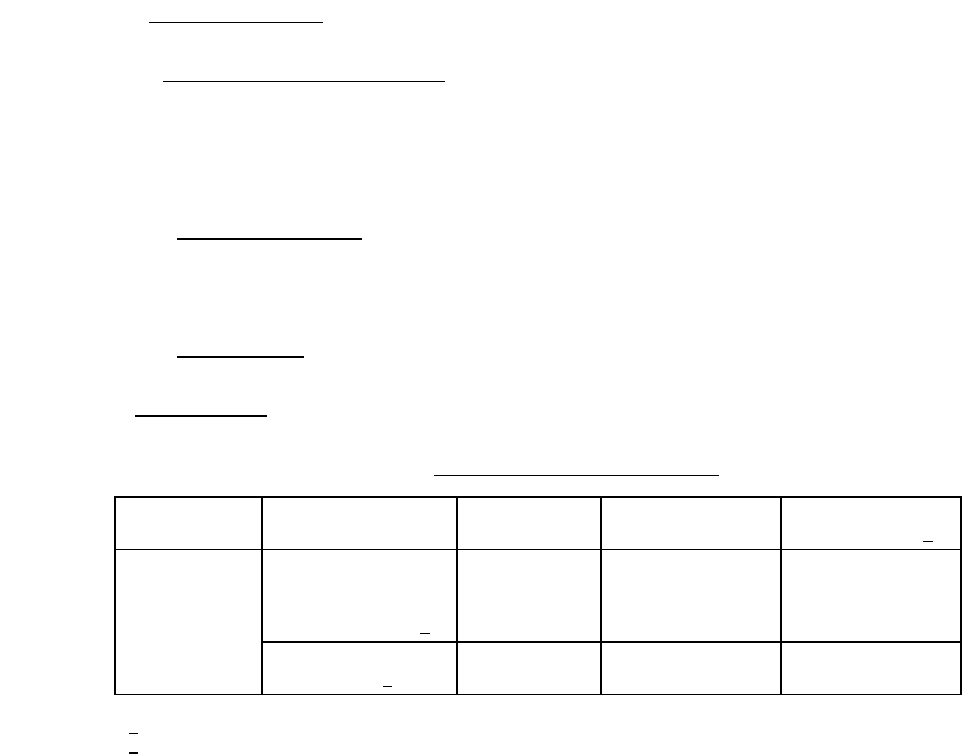
TABLE II. Examination procedure for specimens
.
Device type
Area of
examination
Examination Minimum-maximum
magnification
Photographic
documentation 1
/
Integrated
circuit devices
Passivation steps
(contact windows and
other types of
passivation steps) 2
/
At least one of
each type of
passivation
step present
5,000X to 50,000X Two of the worst
case passivation
steps
General
metallization 2
/
25 percent 1,000X to 6,000X Worst case general
metallization
1
/ See 3.8 (an additional photograph may be required).
2
/ See 3.7 for accept/reject criteria.
*
*
*
*
*