MIL- STD-883F 2004 TEST METHOD STANDARD MICROCIRCUITS.pdf - 第460页
MIL-STD-883F METHOD 2032.2 18 June 2004 54 Cla ss H Class K 3.2.4 Tr immed thic k fi lm res ist or defec ts, "low magnific ation" . No element shall be ac cept able that exhibits : NOTE: The tr im defec t cr it…
MIL-STD-883F
METHOD 2032.2
18 June 2004
53
Class H Class K
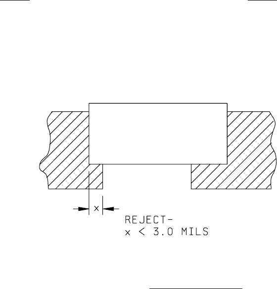
3.2.3 l. Contact overlap between the metallization and 3.2.3 l. Same as class H.
the resistor in which the length
dimension "x" is less than 3.0 mils (see
figure 2032-50h).
FIGURE 2032-50h. Resistor overlap criterion
.
m. Voids or misalignment of glassivation m. Same as class H.
that results in less than 90 percent
coverage of the resistor area, unless
by design.
n. Crazing of glassivation over a resistor. n. Same as class H.
o. Glassivation scratches, lifting, or o. Same as class H.
peeling that expose any portion of a resistor.
MIL-STD-883F
METHOD 2032.2
18 June 2004
54
Class H Class K
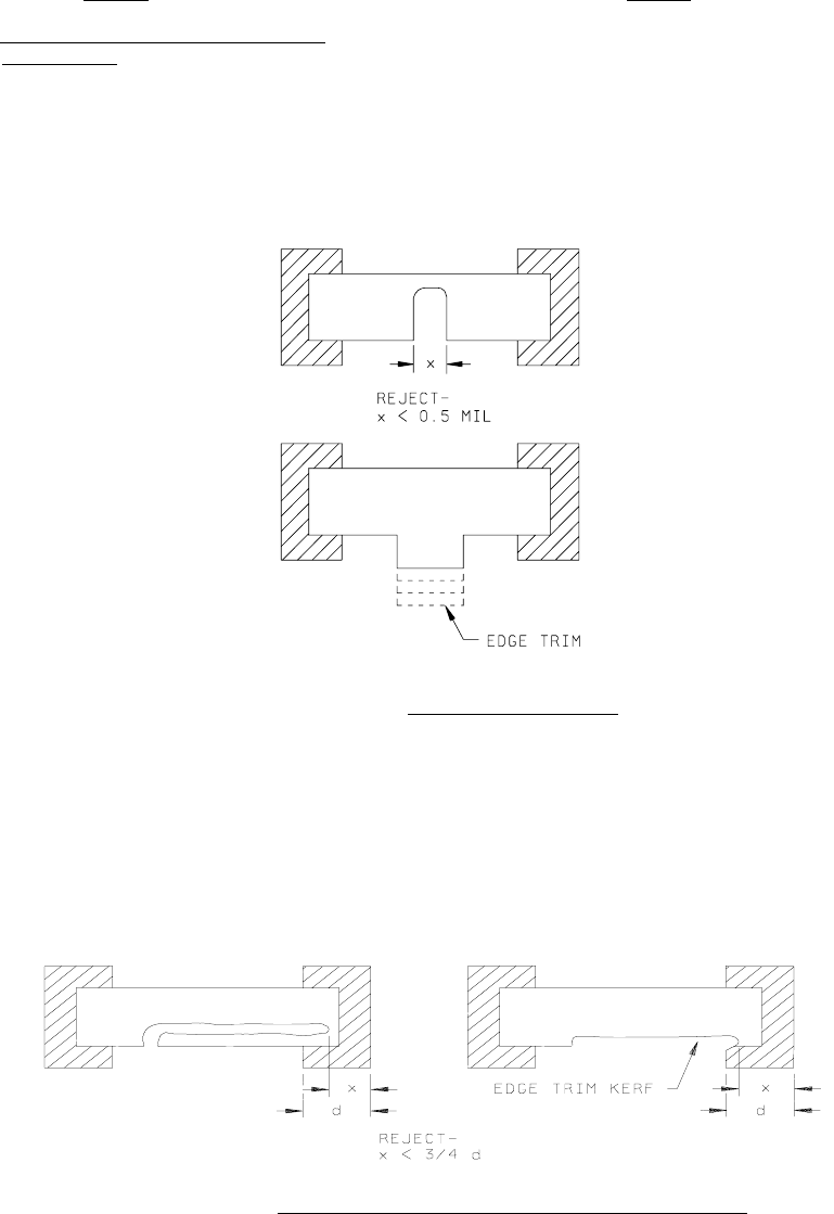
3.2.4 Trimmed thick film resistor defects, "low
magnification"
. No element shall be acceptable that
exhibits:
NOTE: The trim defect criteria contained in this
section apply to active resistor areas only.
a. A kerf width less than 0.5 mil (see figure a. Same as class H.
2032-51h).
NOTE: This does not apply to edge trimming.
FIGURE 2032-51h. Class H kerf width criteria
.
b. A kerf containing detritus. b. Same as class H.
c. A kerf which extends into metallization c. Same as class H.
and leave less than 75 percent of
the metallization width undisturbed
(see figure 2032-52h).
NOTE: Opening a metallization link by
design is acceptable.
FIGURE 2032-52h. Class H laser trim kerf extension into metallization criteria
.
MIL-STD-883F
METHOD 2032.2
18 June 2004
55
Class H Class K
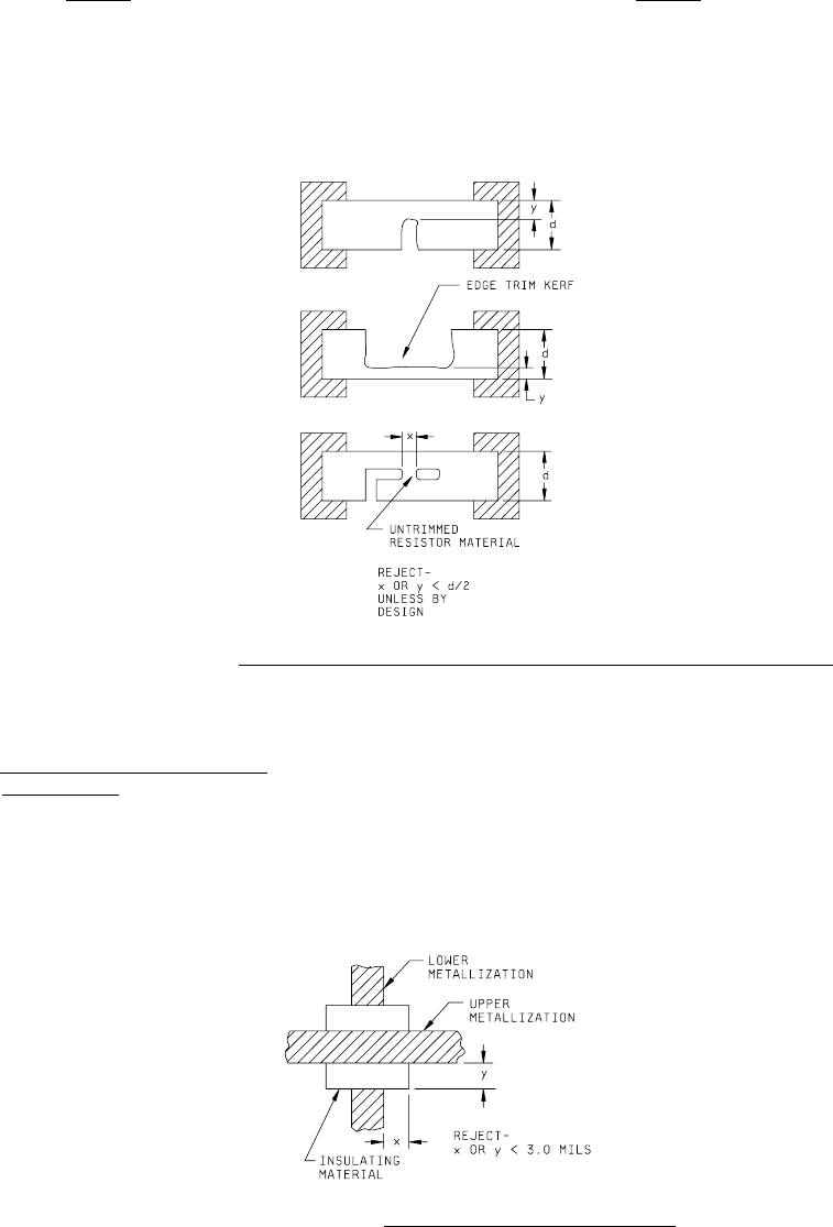
3.2.4 d. A kerf that leaves less than 50 percent 3.2.4 d. Same as class H.
of the original width of a resistor,
unless by design (see figure 2032-52Ah).
PRECAUTIONARY NOTE: The maximum allowable
current density requirement shall not be exceeded.
FIGURE 2032-52Ah. Class H resistor width reduction and untrimmed resistor material criteria
.
e. A trim that does not originate from the edge e. Same as class H.
of the resistor.
3.2.5 Multilevel thick film defects, "low
magnification"
. No element shall be acceptable
that exhibits:
a. Any insulating material that does not a. Same as class H.
extend beyond the width of the upper and
lower metallization by 3.0 mils minimum
(see figure 2032-53h).
FIGURE 2032-53h. Class H dielectric extension criteria
.