MIL- STD-883F 2004 TEST METHOD STANDARD MICROCIRCUITS.pdf - 第273页
MIL-STD-883F METHOD 2012.7 1 June 1993 7 FIGURE 2012-1. Partic le loc ations , pigtai ls, trimmi ng wires , and voids .
MIL-STD-883F
METHOD 2012.7
1 June 1993
6
d. Excessive undercutting of the electrical elements (X and Z plane only, see figure 2012-4).
e. Defective seal: Any device wherein the integral lid seal is not continuous or is reduced from its designed sealing
width by more than 75 percent. Expulsion resulting from the final sealing operation is not considered extraneous
material as long as it can be established that it is continuous, uniform and attached to the parent material and does
not exhibit a ball, splash or tear-drop configuration (i.e., where the base support least dimension is smaller than the
dimension it is supposed to support).
f. Inadequate clearance: Acceptable devices shall have adequate internal clearance to assure that the elements
cannot contact one another or the case. No crossover shall be allowed except as permitted by 3.2.2e of method
2010 (condition A). Depending upon the case type, devices shall be rejected for the following conditions:
NOTE: Any of the following criteria for bond wires shall not apply, if the wires are not visible In the X-ray.
(1) Flat pack and dual-in-line (see figure 2012-5).
(a) Any lead wire that appears to touch or cross another lead wire or bond, (Y plane only).
(b) Any lead wire that deviates from a straight line from bond to external lead and appears to be
within 0.05 mm (.002 inch) of another bond or lead wire (Y plane only).
(c) Lead wires that do not deviate from a straight line from bond to external lead and appear to
touch another wire or bond, excluding common wires, (Y plane only).
(d) Any lead wire that touches or comes within 0.05 mm (0.002 inch) of the case or external lead
to which it is not attached (X and Y plane).
(e) Any bond that is less than 0.025 mm (0.001 inch) (excluding bonds connected by a common
conductor) from another bond (Y plane only).
(f) Any wire making a straight line run from die bonding pad to package post that has no arc.
(g) Lead wires that sag below an imaginary plane across the top of the die bond (X plane only)
except by design.
(2) Round or "box" transistor type (see figure 2012-6).
(a) Any lead wire that touches or comes within 0.05 mm (0.002 inch) of the case or external lead
to which it is not attached (X and Y plane).
(b) Lead wires that sag below an imaginary plane across the top of the die bond (X plane only)
except by design.
(c) Any lead wire that appears to touch or cross another lead wire or bond (Y plane only).
(d) Any lead wire that deviates from a straight line from bond to external lead and appears to
touch or to be within 0.05 mm (0.002 inch) of another wire or bond (Y plane only).
(e) Any bond that is less than 0.025 mm (0.001 inch) (excluding bonds connected by a common
conductor) from another bond (Y plane only).
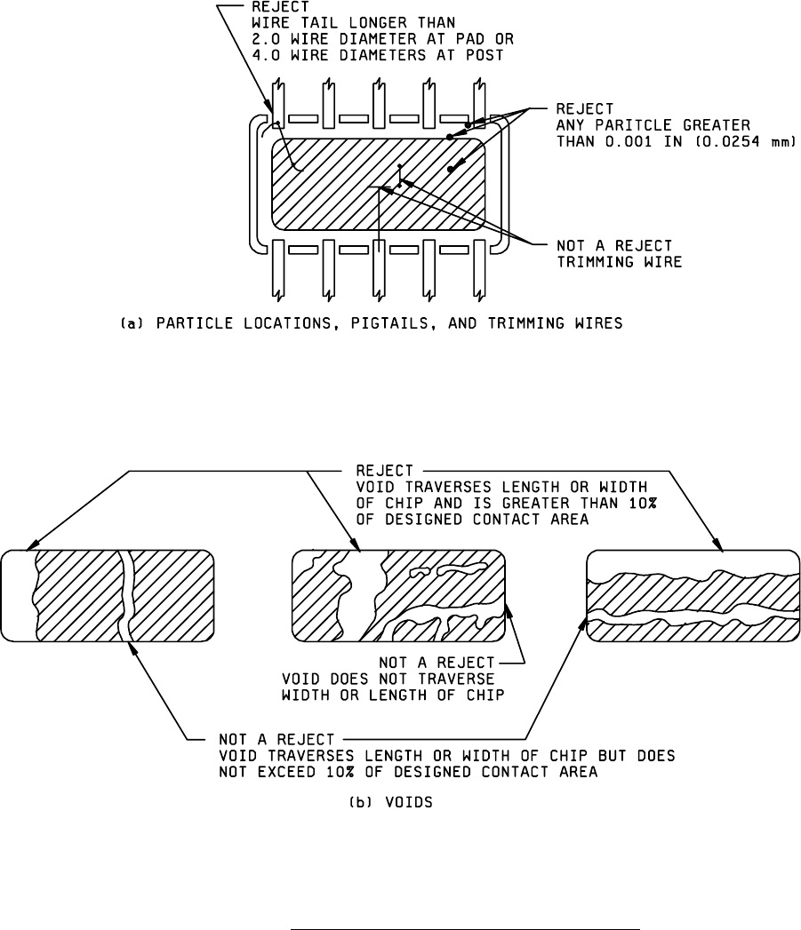
MIL-STD-883F
METHOD 2012.7
1 June 1993
7
FIGURE 2012-1. Particle locations, pigtails, trimming wires, and voids
.
MIL-STD-883F
METHOD 2012.7
1 June 1993
8
(f) Any wire making a straight line run from die bonding pad to package post that has no arc,
unless specifically designed in this manner (e.g., clips or rigid connecting leads).
(g) Any internal post that is bent more than 10° from the vertical (or intended design position) or is
not uniform in length and construction or comes closer than one post diameter to another post.
(h) Where a low profile case (such as TO-46) is used, any post which comes closer to the top of
the case than 20 percent of the total inside dimension between the header and the top of the
case. In devices which have the semiconductor element vertical to the header, any device
where the semiconductor element comes closer than 0.05 mm (0.002 inch) to the header or to
any part of the case.
(i) Any case which does not have a header design incorporating a header edge or other feature
(e.g., a "splash ring") to prevent solder or weld splash from entering the interior of the case.
(3) Cylindrical axial lead type (see figure 2012-8).
(a) Whisker to case distance less than one-half of the diameter of the external lead wire.
(b) Distance from case to semiconductor die or to any eutectic bonding material less than 0.05
mm (0.002 inch).
(c) Whisker tilted more than 5° in any direction from the device lead axis or deformed to the
extent that it touches itself.
(d) C and S shaped whisker with air gap between any two points on it less than twice the
diameter or thickness of the whisker wire. On diodes with whiskers metallurgically bonded to
the post and to the die, the whisker may be deformed to the extent that it touches itself if the
minimum whisker clearance zone specified in figure 2012-8 (a) is maintained.
(e) Whiskerless construction device with anode and cathode lead connections displaced more
than 0.25 mm (0.01 inch) with respect to the central axis of the device.
(f) Semiconductor element mounting tilted more than 15° from normal to the main axis of the
device.
(g) Die hanging over edge of header or pedestal more than 10 percent of the die area.
(h) Less than 75 percent of the semiconductor element base area is bonded to the mounting
surface.
(i) Voids in the welds, from any edge, between the leads and the heat sink slugs greater than 15
percent of the lead wire diameter. Any voids whatever in the central part of the area that
should be welded.
(j) Devices with package deformities such as, body glass cracks, incomplete seals (voids,
position glass, etc), die chip outs and severe misalignment of S and C shaped whisker
connections to die or post.