S1.pdf - 第4页
Advantages of EUVL : Samsung Infographic Low er patterning cost (limiting multiple exposures) In a full fab, EUV enabl es higher output Slide 4 https://news.samsung.com/global/info graphic-euv-samsungs-latest-investment-…
Slide 3
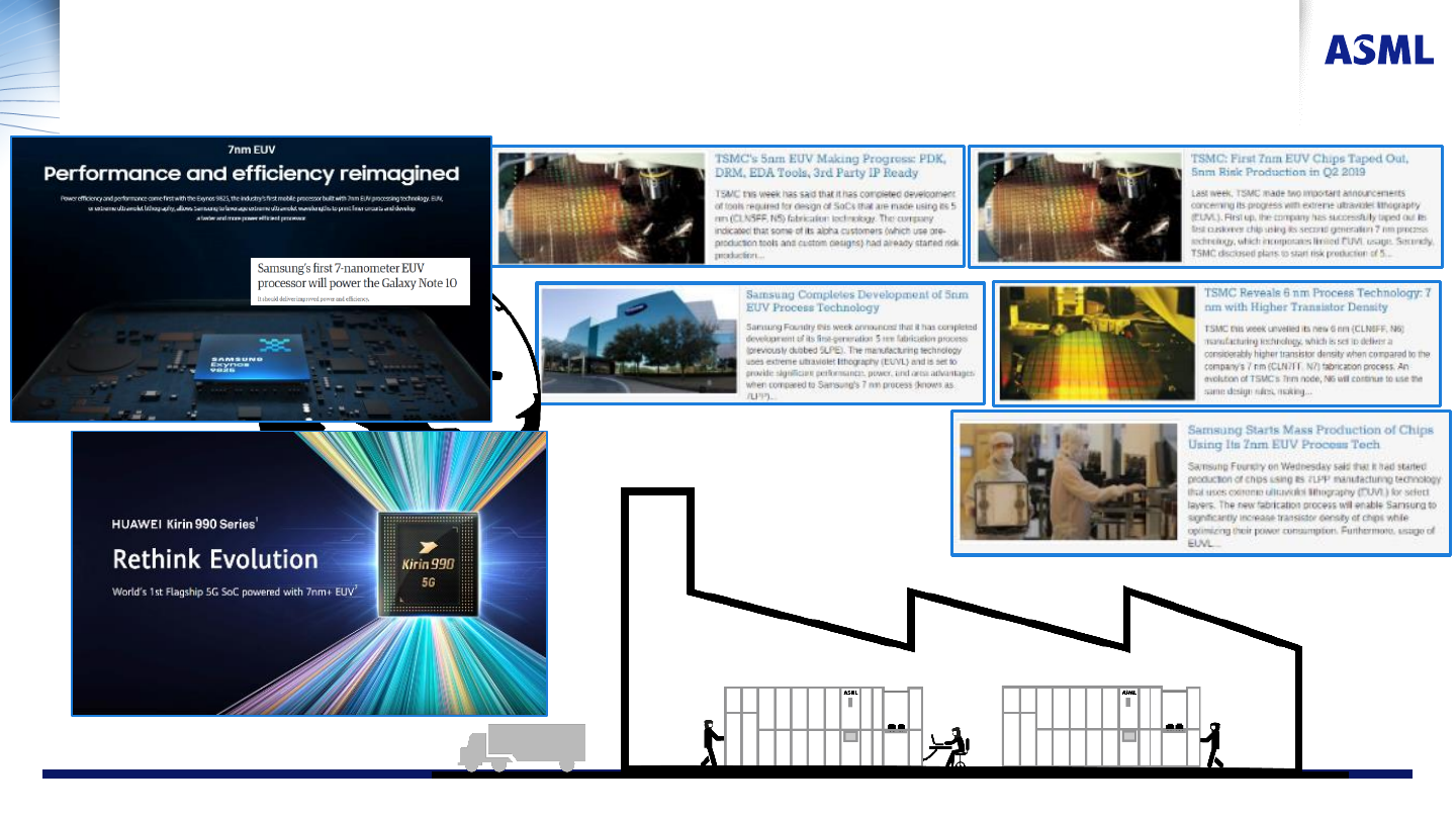
And it’s here: we see EUV - enabled chips in 2019
EUV up and running in High Volume Manufacturing
Public
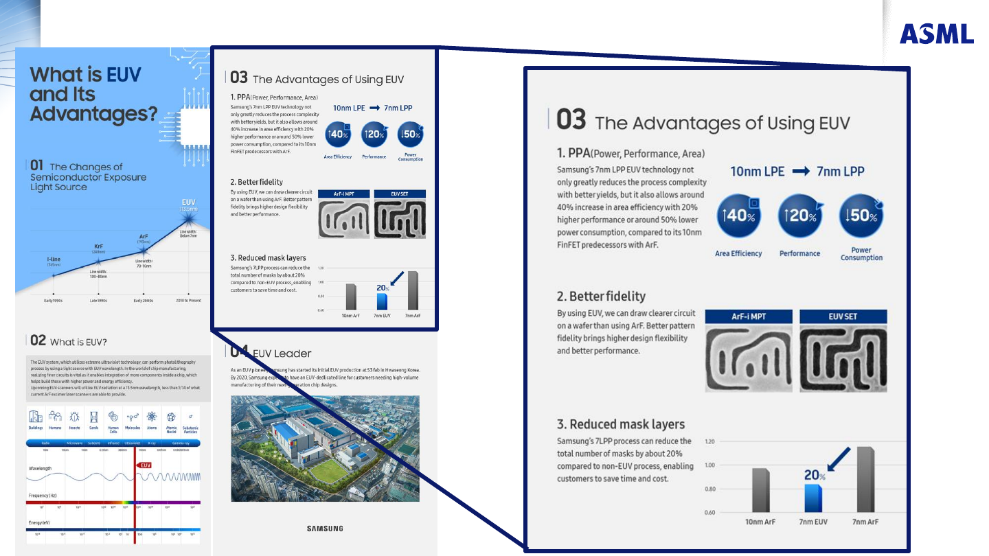
Advantages of EUVL : Samsung Infographic
Lower patterning cost (limiting multiple exposures)
In a full fab, EUV enables higher output
Slide 4
https://news.samsung.com/global/infographic-euv-samsungs-latest-investment-on-developing-next-generation-semiconductor-products
Public
Why EUV? - Resolution in Optical Lithography
Slide 5
Critical Dimension:
Depth of focus:
k: process parameter
NA: numerical aperture
: wavelength of light
KrF-Laser: 248nm
ArF-Laser: 193 nm
ArF-Laser (immersion): 193 nm
EUV sources: 13.5 nm
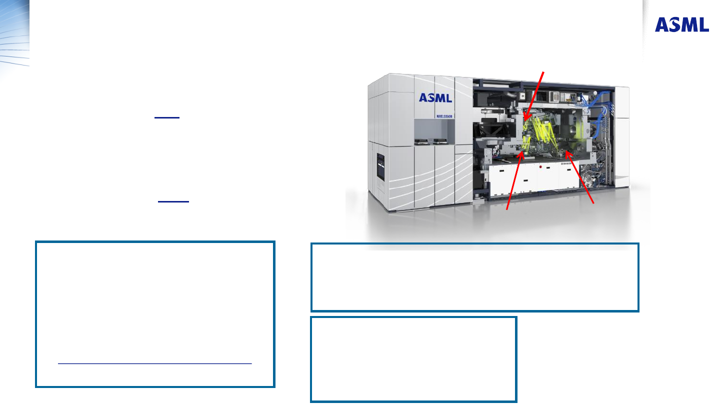
EUV source
Wafer stage
Reticle stage
theoretical limit (air): NA=1
practical limit: NA=0.9
theoretical limit (immersion):NA ≈ n (~1.7)
k
1
is process parameter
traditionally: >0.75
typically: 0.3 – 0.4
theoretical limit: 0.25
Public